Resources
About Us
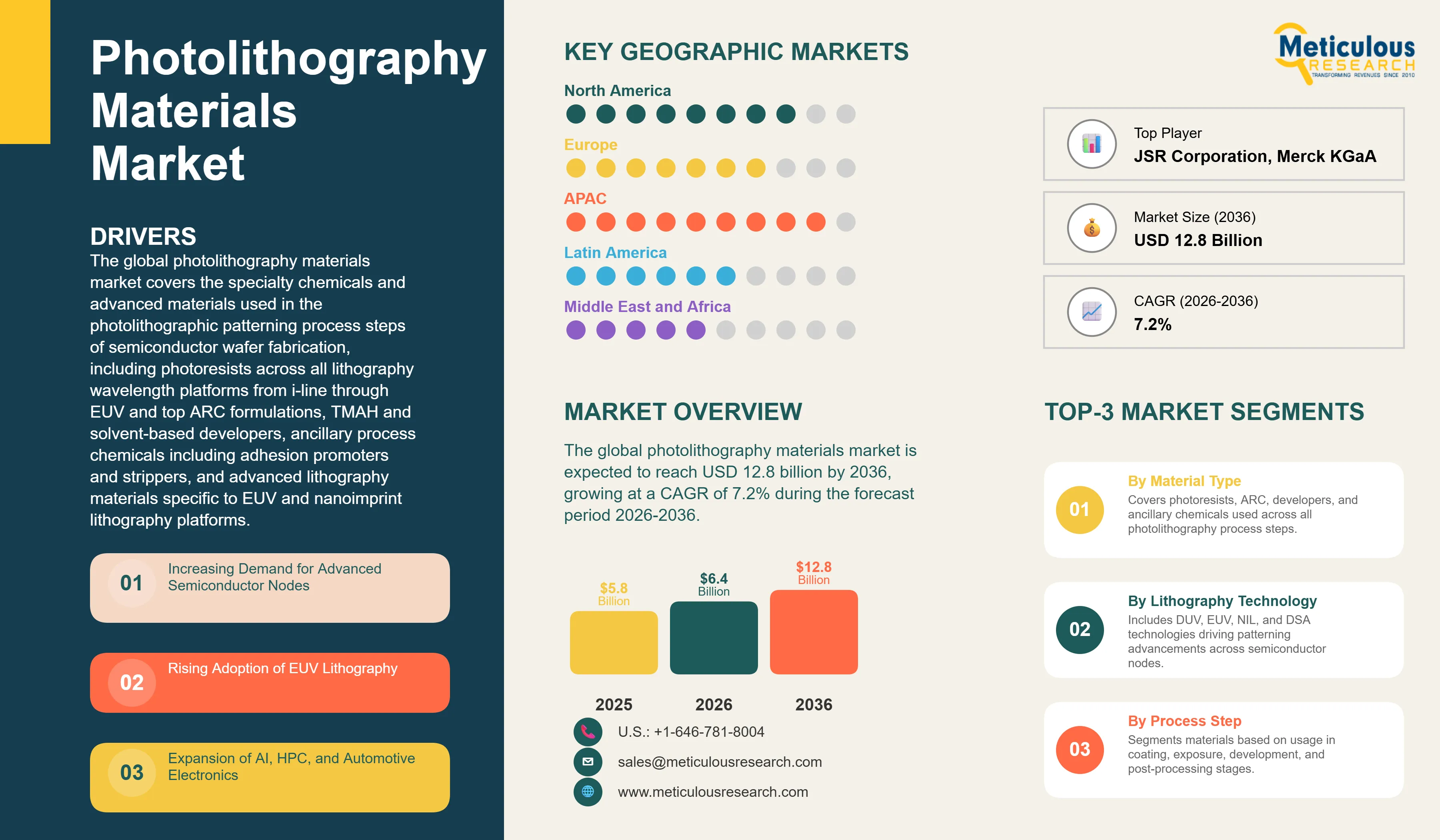
The global photolithography materials market was valued at USD 5.8 billion in 2025. This market is expected to reach USD 12.8 billion by 2036 from an estimated USD 6.4 billion in 2026, growing at a CAGR of 7.2% during the forecast period 2026-2036.
 Click here to: Get Free Sample Pages of this Report
The global photolithography materials market covers the specialty chemicals and advanced materials used in the photolithographic patterning process steps of semiconductor wafer fabrication, including photoresists across all lithography wavelength platforms from i-line through EUV, anti-reflective coatings including bottom ARC and top ARC formulations, TMAH and solvent-based developers, ancillary process chemicals including adhesion promoters, edge bead removers, thinners, and strippers, and advanced lithography materials specific to EUV, directed self-assembly, and nanoimprint lithography platforms. These materials are consumed across every patterned layer in semiconductor chip manufacturing and are critical determinants of the resolution, line edge roughness, defect density, and pattern fidelity that define device performance and manufacturing yield at each technology node.
The growth of the global photolithography materials market is primarily driven by the semiconductor industry's continued advancement along the technology node roadmap toward 3 nm, 2 nm, and sub-2 nm logic nodes that require progressively more sophisticated photoresist chemistries and process materials to achieve the pattern resolution, sensitivity, and defect performance required at leading-edge manufacturing. The rapid expansion of EUV lithography capacity at TSMC, Samsung Foundry, and Intel Foundry is creating strong demand for EUV-specific photoresist chemistries, anti-reflective underlayers, and associated process chemicals engineered for 13.5 nm wavelength exposure, representing the highest-value segment of the photolithography materials market with material costs per wafer layer significantly exceeding DUV equivalents.
Two significant opportunities are shaping the market's long-term trajectory. The progression toward High-NA EUV lithography, with ASML's EXE:5000 scanner entering production at Intel Foundry for its Intel 14A process, is creating demand for next-generation photoresist and underlayer materials specifically engineered for the 0.55 numerical aperture optical system and its tighter depth of focus that requires thinner resist films with enhanced etch resistance and sensitivity. The rapid growth of advanced packaging as a pathway for system performance scaling beyond single-chip transistor density improvements is creating a large and fast-growing new demand channel for photolithography materials in redistribution layer patterning, micro-bump formation, and through-silicon via processes at OSAT facilities and integrated packaging foundries.
|
Parameters |
Details |
|
Market Size by 2036 |
USD 12.8 Billion |
|
Market Size in 2026 |
USD 6.4 Billion |
|
Market Size in 2025 |
USD 5.8 Billion |
|
Revenue Growth Rate (2026-2036) |
CAGR of 7.2% |
|
Dominating Material Type |
Photoresists |
|
Fastest Growing Material Type |
Advanced Lithography Materials (EUV-Specific) |
|
Dominating Lithography Technology |
Deep Ultraviolet (DUV) |
|
Fastest Growing Lithography Technology |
Extreme Ultraviolet (EUV) |
|
Dominating Technology Node |
>=28 nm |
|
Fastest Growing Technology Node |
<=3 nm |
|
Dominating Application |
Foundry |
|
Fastest Growing Application |
Advanced Packaging |
|
Dominating End User |
Foundries |
|
Fastest Growing End User |
OSAT |
|
Dominating Geography |
Asia-Pacific |
|
Fastest Growing Geography |
North America |
|
Base Year |
2025 |
|
Forecast Period |
2026 to 2036 |
Rising Adoption of EUV Lithography and EUV-Specific Materials
The progressive industry-wide transition from DUV multi-patterning to single-exposure EUV lithography for advanced logic and memory nodes represents the most commercially significant structural trend in the global photolithography materials market. EUV lithography at the 5 nm node and below eliminates the need for multiple DUV patterning passes per layer, reducing manufacturing cycle time and cumulative overlay error while enabling the feature resolution and edge placement accuracy required for leading-edge device architecture. TSMC, Samsung Foundry, and Intel Foundry have collectively installed over 200 ASML EUV scanners as of 2025, with annual scanner shipments continuing to increase as these foundries ramp N3, N2, and future sub-2 nm node capacity.
EUV photoresist development represents the most technically demanding material innovation challenge in the photolithography materials industry. EUV resists must simultaneously achieve the very high sensitivity required to minimize absorbed dose per exposure and the extremely low line edge roughness needed for leading-edge device patterning within the fundamental stochastic noise constraints imposed by EUV photon statistics. JSR Corporation's EUV resist programs, Tokyo Ohka Kogyo's EUV chemistry development, Fujifilm's metal-oxide resist platform, and Inpria's tin-oxide EUV resist technology acquired by Merck represent the leading EUV photoresist development programs advancing toward the sensitivity-roughness performance targets required for High-NA EUV compatibility.
Growth in Advanced Packaging Lithography Materials
The rapid expansion of heterogeneous integration and advanced chip packaging as a primary pathway for continued system performance scaling is creating a large and fast-growing new demand segment for photolithography materials in applications that differ technically and commercially from traditional front-end wafer fabrication. Advanced packaging platforms including TSMC's Chip-on-Wafer-on-Substrate and System-on-Integrated-Chips, Samsung's X-Cube, and Intel's Embedded Multi-die Interconnect Bridge require photolithographic patterning of fine-pitch redistribution layers, micro-pillar copper bump arrays, and through-silicon via fill structures at minimum feature dimensions between 2 and 10 micrometers, consuming photoresist, developer, and ancillary chemical formulations optimized for the specific film thicknesses and substrate topographies of packaging process flows.
OSAT companies including ASE Group, Amkor Technology, JCET, and Powertech Technology are investing in advanced packaging lithography capabilities to serve the growing demand for chiplet integration packaging from fabless semiconductor companies and system OEMs seeking heterogeneous integration performance without access to leading-edge logic foundry nodes. This transition is expanding the photolithography materials customer base from the concentrated group of leading-edge foundries and IDMs that have historically dominated market demand to a larger and more diverse ecosystem of packaging facilities that are adopting lithographic patterning for the first time, creating a new growth vector for photolithography material suppliers that broadens the market's revenue base and geographic distribution.
Emerging Semiconductor Manufacturing Regions Driving New Demand Centers
The global diversification of semiconductor manufacturing geography, accelerated by the U.S. CHIPS Act, the EU Chips Act, India's semiconductor incentive programs, and Japan's RAPIDUS national semiconductor initiative, is creating new photolithography material demand centers in regions that have historically consumed minimal volumes of advanced semiconductor manufacturing chemicals. The TSMC Arizona fab complex, Samsung Austin and Taylor fabs, Intel Ohio and Arizona facilities, and Micron's U.S. expansion collectively represent tens of billions of dollars in U.S. semiconductor manufacturing investment that will require domestic or nearby-sourced photolithography material supply chains to satisfy CHIPS Act compliance requirements and minimize logistics disruption risk.
European semiconductor manufacturing expansion through Intel's Magdeburg fab, TSMC Dresden joint venture with Bosch, Infineon, and NXP, and STMicroelectronics' European capacity expansions are creating growing European photolithography material demand for which regional suppliers including Merck KGaA are well-positioned through their existing semiconductor materials business and European manufacturing infrastructure. Japan's RAPIDUS program targeting sub-2 nm logic manufacturing at Chitose with IBM technology collaboration is driving photolithography material development partnerships with Japanese specialty chemical companies including JSR, Tokyo Ohka Kogyo, and Shin-Etsu Chemical that have decades of deep technical collaboration with Japanese and global semiconductor manufacturers.
Increasing Demand for Advanced Semiconductor Nodes
The semiconductor industry's continued advancement toward sub-3 nm and sub-2 nm logic nodes is the primary structural driver of the photolithography materials market, as each successive technology node generation requires new or substantially reformulated photoresist chemistries, anti-reflective coating architectures, and ancillary process chemicals engineered to meet the tighter resolution, line edge roughness, defect density, and etch selectivity specifications of the smaller feature dimensions and more complex multi-layer patterning schemes required at leading-edge nodes. The transition from DUV multi-patterning to EUV single exposure and the progression toward High-NA EUV for sub-2 nm nodes each represent step-change increases in photolithography material performance requirements that create commercial opportunities for material suppliers with the R&D capability to develop qualified products meeting the new specifications. The computing semiconductor demand driven by AI accelerator chip production, the memory demand driven by high-bandwidth memory for AI systems, and the logic demand driven by smartphone and PC application processor advancement are all sustaining leading-edge node fabrication investment and the associated photolithography material demand.
Growing Global Fab Investments
The unprecedented wave of semiconductor fabrication investment being driven by the U.S. CHIPS and Science Act, the EU Chips Act, Japan's semiconductor reindustrialization programs, India's semiconductor incentive scheme, and the parallel capacity expansion programs of TSMC, Samsung, Intel, Micron, SK Hynix, and domestic Chinese manufacturers is creating the largest sustained increase in global wafer fabrication capacity in semiconductor industry history. New fab construction investments of several hundred billion dollars collectively announced for the 2024 to 2030 period represent direct capital expenditure programs that will require photolithography materials procurement at every production stage from facility qualification and process development through full-volume production ramp. Each new advanced logic or memory fab entering production represents a sustained and growing annual photolithography material procurement program extending across the facility's multi-decade operational lifetime, providing long-term revenue visibility for qualified photolithography material suppliers contracted to supply new manufacturing programs.
Development of High-NA EUV Materials
The commercial introduction of ASML's High-NA EUV scanner platform, the EXE:5000 series with 0.55 numerical aperture, represents the most significant photolithography technology transition since the original EUV adoption and creates a major new material development opportunity for photoresist and underlayer suppliers capable of qualifying products meeting the demanding performance requirements of the High-NA exposure environment. High-NA EUV's tighter depth of focus compared with Low-NA EUV requires significantly thinner photoresist films, typically below 30 nanometers compared with 40 to 50 nanometers for Low-NA EUV, that must simultaneously provide sufficient etch resistance to survive pattern transfer into underlying substrate layers. This thin-film performance requirement is driving development of metal-oxide photoresist platforms including the tin-oxide chemistry developed by Inpria and now advanced by Merck, organometallic resist compositions, and novel molecular glass resist architectures that can achieve the required sensitivity and line edge roughness performance at extremely thin film thicknesses. Material suppliers that successfully qualify High-NA EUV compatible products will access a premium-priced and initially capacity-constrained market segment at the leading edge of semiconductor technology.
Growth in Advanced Packaging Lithography
The rapid growth of advanced packaging as a semiconductor performance scaling pathway independent of transistor density advancement is creating a substantial and expanding addressable market for photolithography materials in packaging process applications that differ in technical requirements, customer base, and geographic distribution from traditional front-end wafer fabrication material consumption. Redistribution layer patterning for fan-out wafer-level and panel-level packaging, micro-pillar copper bump formation for flip-chip and 3D stacking, and through-silicon via reveal and isolation processes all require photoresist, ARC, developer, and ancillary chemical formulations qualified for the specific process conditions, substrate materials, and feature dimension requirements of advanced packaging workflows. The expanding OSAT packaging customer base, growing from a handful of leading foundries to a broader ecosystem of packaging specialists, provides material suppliers with a more diversified and geographically distributed demand base that reduces concentration risk relative to the highly consolidated leading-edge logic foundry customer segment.
By Material Type: In 2026, Photoresists to Dominate
Based on material type, the global photolithography materials market is segmented into photoresists, anti-reflective coatings, developers, ancillary chemicals, advanced lithography materials, and other photolithography materials. In 2026, the photoresists segment is expected to account for the largest share of the global photolithography materials market. The large share of this segment is attributed to photoresists representing the primary functional patterning material applied at every photolithographic layer in wafer fabrication, the high dollar value per unit volume of advanced DUV and EUV photoresist formulations that can cost several thousand dollars per liter for leading-edge EUV products, and the broad consumption base spanning legacy i-line and KrF photoresists used in mature node production through ArF immersion resists at 7 to 14 nm and EUV resists at 5 nm and below. JSR Corporation, Tokyo Ohka Kogyo, Shin-Etsu Chemical, Fujifilm, and Sumitomo Chemical collectively supply the large majority of the global photoresist market.
However, the advanced lithography materials segment is poised to register the highest CAGR during the forecast period. The high growth of this segment is attributed to the accelerating expansion of EUV lithography capacity at leading foundries driving demand for EUV-specific underlayer and topcoat materials, the commercial introduction of High-NA EUV driving a new generation of resist and process material development, and the increasing commercial activity in directed self-assembly and nanoimprint lithography material platforms targeting specific advanced patterning applications.
By Lithography Technology: In 2026, DUV to Hold the Largest Share
Based on lithography technology, the global photolithography materials market is segmented into deep ultraviolet (DUV), extreme ultraviolet (EUV), nanoimprint lithography (NIL), and directed self-assembly (DSA). In 2026, the DUV segment is expected to account for the largest share of the global photolithography materials market. This dominance reflects the vast installed base of DUV lithography scanners globally spanning KrF, ArF dry, and ArF immersion platforms that serve the full range of semiconductor manufacturing from legacy mature nodes through leading-edge 7 nm production via multi-patterning, generating very large and sustained photoresist, ARC, and developer material consumption volumes across thousands of production scanner tools at foundries and IDMs worldwide.
However, the EUV segment is projected to register the highest CAGR during the forecast period. This growth is driven by the continued rapid expansion of EUV scanner installations at TSMC, Samsung Foundry, and Intel Foundry for advanced logic production and the ramp of EUV in DRAM manufacturing at Samsung, SK Hynix, and Micron for sub-1z and sub-1alpha DRAM nodes, each new scanner installation representing sustained annual photoresist and process chemical consumption at EUV material pricing levels substantially above DUV equivalents.
By Technology Node: In 2026, the >=28 nm Segment to Hold the Largest Share
Based on technology node, the global photolithography materials market is segmented into 28 nm and above, 14 to 28 nm, 7 to 14 nm, 7 nm and below, and 3 nm and below. In 2026, the 28 nm and above segment is expected to account for the largest share of the global photolithography materials market by consumption volume, as legacy and mature node semiconductor manufacturing at 28 nm, 40 nm, 65 nm, 90 nm, and above collectively represents the largest installed base of semiconductor fabrication capacity globally and generates very high aggregate photolithography material consumption volumes across the thousands of mature node wafer starts processed monthly at high-volume manufacturing facilities worldwide, including the rapidly expanding mature node capacity being built in China.
However, the 3 nm and below segment is projected to register the highest CAGR during the forecast period. This growth is driven by the advancing production ramp of TSMC's N3 and N2 node families, Samsung Foundry's 3GAE and 2 nm SF2 processes, and Intel Foundry's Intel 18A and future Intel 14A platforms, all of which use multiple EUV exposure layers per chip manufacturing flow and consume photolithography materials at the highest per-wafer value intensity of any technology node generation, supporting very high revenue growth despite more modest wafer volume growth compared with mature nodes.
By Application: In 2026, Foundry to Hold the Largest Share
Based on application, the global photolithography materials market is segmented into logic, memory (DRAM and NAND), foundry, and advanced packaging. In 2026, the foundry segment is expected to account for the largest share of the global photolithography materials market. This dominance reflects pure-play foundries' dominant and increasing share of global semiconductor manufacturing capacity, anchored by TSMC's leading market position supplying the large majority of the world's most advanced logic chip production for Apple, NVIDIA, AMD, Qualcomm, and MediaTek, and the growing capacity of Samsung Foundry, GlobalFoundries, UMC, and SMIC collectively representing a large and growing photolithography material consumption base across all technology nodes from mature to leading-edge.
However, the advanced packaging segment is projected to register the highest CAGR during the forecast period. This growth is driven by the rapid adoption of photolithography-based redistribution layer patterning and micro-bump formation in advanced packaging workflows by OSAT companies and integrated packaging foundries, the growing volume of AI accelerator chiplet packages and high-bandwidth memory stacks requiring fine-pitch interconnect lithography, and the progressive expansion of advanced packaging from a small number of leading-edge applications toward broader semiconductor assembly production that is progressively displacing conventional wire bond and flip-chip packaging in new design starts.
By End User: In 2026, Foundries to Hold the Largest Share
Based on end user, the global photolithography materials market is segmented into integrated device manufacturers (IDMs), foundries, and OSAT companies. In 2026, the foundries segment is expected to account for the largest share of the global photolithography materials market. Pure-play foundries represent the dominant photolithography material consumption channel, as their business model of manufacturing chips for fabless semiconductor companies across the full range of technology nodes from legacy through leading-edge generates high-volume, continuous material procurement programs that constitute the primary revenue base for photolithography material suppliers. TSMC alone, as the world's largest semiconductor foundry with over 50% of global foundry revenue, represents an extraordinary concentration of photolithography material demand that makes it the single most important customer account for the majority of photoresist and specialty chemical suppliers serving the semiconductor industry.
However, the OSAT segment is projected to register the highest CAGR during the forecast period. This growth is driven by OSAT companies' rapid adoption of advanced packaging processes requiring photolithographic patterning, creating new photolithography material demand at packaging facilities that have historically required only wire bond and conventional flip-chip assembly chemicals. The expanding OSAT advanced packaging capacity investment programs of ASE Group, Amkor Technology, JCET, and Powertech Technology in response to AI package demand are establishing a new and growing photolithography material consumption base within the OSAT segment.
Photolithography Materials Market by Region: Asia-Pacific Leading by Share, North America by Growth
Based on geography, the global photolithography materials market is segmented into Asia-Pacific, North America, Europe, Latin America, and the Middle East and Africa.
In 2026, Asia-Pacific is expected to account for the largest share of the global photolithography materials market. The largest share of this region is mainly due to the concentration of the world's leading semiconductor foundries and IDMs in Taiwan, South Korea, Japan, and China, which collectively process the large majority of global semiconductor wafer output and therefore consume the largest share of photolithography materials across all technology generations. TSMC's multiple Hsinchu, Taichung, Tainan, and Kaohsiung fab complexes in Taiwan collectively represent the largest single-country photolithography material consumption base globally, followed by Samsung's Hwaseong, Pyeongtaek, and Giheung complexes and SK Hynix's Icheon and Cheongju facilities in South Korea. Japan's photolithography materials market benefits from both the domestic consumption of Sony Semiconductor, Kioxia, and Renesas manufacturing facilities and the dominant role of Japanese photoresist and specialty chemical suppliers including JSR, Tokyo Ohka Kogyo, Shin-Etsu Chemical, and Fujifilm that serve global semiconductor manufacturers from Japanese production bases. China's photolithography material demand is growing rapidly as SMIC, CXMT, and YMTC expand domestic semiconductor manufacturing capacity at mature and mid-range technology nodes.
However, the North American photolithography materials market is expected to grow at the fastest CAGR during the forecast period. North America's rapid growth is driven by the unprecedented wave of semiconductor manufacturing investment catalyzed by the CHIPS and Science Act's USD 52 billion in semiconductor manufacturing incentives, which is bringing TSMC's three-fab Arizona complex, Samsung's Taylor and Austin Texas facilities, Intel's Ohio, Arizona, and New Mexico facilities, Micron's Idaho and New York memory fabs, and GlobalFoundries' U.S. capacity expansions into production over the 2025 to 2030 period. These new facilities collectively represent tens of gigawatts of additional U.S. semiconductor manufacturing capacity that will require sustained photolithography material supply streams, creating a large new North American photolithography material demand center that global suppliers including JSR, Tokyo Ohka Kogyo, Merck, DuPont, Brewer Science, and Avantor are investing to serve through U.S. manufacturing and distribution capacity expansion.
Europe's photolithography materials market is supported by the strong domestic semiconductor specialty chemical industry anchored by Merck KGaA's Semiconductor Solutions division in Darmstadt, BASF's electronic materials business, and the photoresist and ARC activities of regional specialty chemical producers, as well as the growing European semiconductor manufacturing base including ASML's EUV scanner manufacturing in Veldhoven that positions the Netherlands as a center of EUV ecosystem activity. The EU Chips Act's EUR 43 billion investment mobilization program is supporting fab expansions by Intel in Magdeburg, TSMC in Dresden, Infineon in Austria, and STMicroelectronics across multiple European sites that will increase European photolithography material consumption through the forecast period.
The global photolithography materials market is highly concentrated at the photoresist tier, where a small number of Japanese and U.S. specialty chemical companies hold strong technology and market share positions based on decades of co-development with semiconductor manufacturers and deep integration into fab qualification and process development programs. Competition is focused on photoresist chemistry performance differentiation, particularly EUV and High-NA EUV sensitivity and roughness performance, supply security, chemical purity levels meeting sub-ppb metal contamination specifications, and the technical service capabilities required to support material qualification at leading-edge nodes.
The report provides a comprehensive competitive analysis based on an extensive assessment of leading players' product portfolios, technology development programs, geographic presence, and key strategic developments. Some of the key players operating in the global photolithography materials market include JSR Corporation (Japan), Tokyo Ohka Kogyo Co. Ltd. (Japan), Shin-Etsu Chemical Co. Ltd. (Japan), Fujifilm Holdings Corporation (Japan), Merck KGaA (Germany), DuPont de Nemours Inc. (U.S.), Sumitomo Chemical Co. Ltd. (Japan), Dongjin Semichem Co. Ltd. (South Korea), LG Chem Ltd. (South Korea), Samsung SDI Co. Ltd. (South Korea), BASF SE (Germany), Cabot Microelectronics (U.S.), Avantor Inc. (U.S.), Brewer Science Inc. (U.S.), and Allresist GmbH (Germany), among others.
The global photolithography materials market is expected to reach USD 12.8 billion by 2036 from an estimated USD 6.4 billion in 2026, at a CAGR of 7.2% during the forecast period 2026-2036.
In 2026, the photoresists segment is expected to hold the largest share of the global photolithography materials market, driven by photoresists' role as the primary functional patterning material at every lithographic layer and the high dollar value per unit volume of advanced DUV and EUV photoresist formulations.
The advanced lithography materials segment is expected to register the highest CAGR during the forecast period 2026-2036, driven by the accelerating expansion of EUV lithography capacity at leading foundries and the commercial introduction of High-NA EUV creating demand for next-generation resist and underlayer chemistries.
In 2026, the DUV segment is expected to hold the largest share of the global photolithography materials market, reflecting the vast installed base of DUV scanners globally serving mature through leading-edge 7 nm semiconductor manufacturing via multi-patterning.
In 2026, the foundry segment is expected to hold the largest share of the global photolithography materials market, reflecting pure-play foundries' dominant position in global semiconductor manufacturing capacity and the concentration of leading-edge material consumption at major foundry accounts.
The growth of this market is primarily driven by the semiconductor industry's continued advancement to sub-3 nm and sub-2 nm logic nodes requiring progressively more sophisticated EUV photoresist and process chemistries, and the unprecedented global wave of semiconductor fab investment catalyzed by the U.S. CHIPS Act, EU Chips Act, and national semiconductor programs in Japan, South Korea, and India that are creating large new photolithography material demand centers across multiple regions simultaneously.
Key players are JSR Corporation (Japan), Tokyo Ohka Kogyo Co. Ltd. (Japan), Shin-Etsu Chemical Co. Ltd. (Japan), Fujifilm Holdings Corporation (Japan), Merck KGaA (Germany), DuPont de Nemours Inc. (U.S.), Sumitomo Chemical Co. Ltd. (Japan), Dongjin Semichem Co. Ltd. (South Korea), LG Chem Ltd. (South Korea), Samsung SDI Co. Ltd. (South Korea), BASF SE (Germany), Cabot Microelectronics (U.S.), Avantor Inc. (U.S.), Brewer Science Inc. (U.S.), and Allresist GmbH (Germany), among others.
North America is expected to register the highest growth rate in the global photolithography materials market during the forecast period 2026-2036, driven by the U.S. CHIPS Act-catalyzed wave of fab construction by TSMC, Samsung, Intel, and Micron creating large new domestic photolithography material demand centers.
1. Introduction
1.1 Market Definition
1.2 Market Ecosystem
1.3 Currency and Limitations
1.3.1 Currency
1.3.2 Limitations
1.4 Key Stakeholders
2. Research Methodology
2.1 Research Approach
2.2 Data Collection & Validation Process
2.2.1 Secondary Research
2.2.2 Primary Research & Validation
2.2.2.1 Primary Interviews with Experts
2.2.2.2 Approaches for Country-/Region-Level Analysis
2.3 Market Estimation
2.3.1 Bottom-Up Approach
2.3.2 Top-Down Approach
2.3.3 Growth Forecast
2.4 Data Triangulation
2.5 Assumptions for the Study
3. Executive Summary
4. Market Overview
4.1 Introduction
4.2 Market Dynamics
4.2.1 Drivers
4.2.1.1 Increasing Demand for Advanced Semiconductor Nodes
4.2.1.2 Rising Adoption of EUV Lithography
4.2.1.3 Expansion of AI, HPC, and Automotive Electronics
4.2.1.4 Growing Global Fab Investments
4.2.2 Restraints
4.2.2.1 High Cost of EUV Materials
4.2.2.2 Long Qualification Cycles
4.2.2.3 Supply Chain Concentration
4.2.3 Opportunities
4.2.3.1 Development of High-NA EUV Materials
4.2.3.2 Growth in Advanced Packaging Lithography
4.2.3.3 Emerging Semiconductor Manufacturing Regions
4.2.3.4 Innovation in Multi-Patterning Techniques
4.2.4 Challenges
4.2.4.1 Line Edge Roughness and Defect Control
4.2.4.2 Sensitivity vs Resolution Trade-offs
4.3 Technology Landscape
4.3.1 DUV Lithography (KrF, ArF)
4.3.2 EUV Lithography
4.3.3 Nanoimprint Lithography (NIL)
4.3.4 Directed Self-Assembly (DSA)
4.4 Photolithography Process Architecture
4.4.1 Surface Preparation & Adhesion
4.4.2 Photoresist Coating
4.4.3 Exposure (DUV/EUV)
4.4.4 Post-Exposure Bake (PEB)
4.4.5 Development
4.4.6 Pattern Transfer Support
4.5 Value Chain Analysis
4.5.1 Raw Material Suppliers
4.5.2 Material Manufacturers
4.5.3 Semiconductor Foundries & IDMs
4.5.4 Equipment Manufacturers
4.5.5 End Users
4.6 Regulatory and Standards Landscape
4.6.1 Chemical Purity Standards
4.6.2 Environmental Regulations
4.6.3 Semiconductor Manufacturing Standards
4.7 Porter's Five Forces Analysis
4.8 Investment and Capacity Expansion Analysis
4.8.1 Fab Expansion Trends
4.8.2 EUV Adoption Investments
4.8.3 Strategic Collaborations
4.9 Cost and Pricing Analysis
4.9.1 Cost Structure by Material Type
4.9.2 EUV vs DUV Pricing Comparison
4.9.3 Pricing by Node and Purity
5. Photolithography Materials Market, by Material Type (Primary Segmentation)
5.1 Introduction
5.2 Photoresists
5.2.1 Chemically Amplified Resists (CAR)
5.2.2 Non-Chemically Amplified Resists
5.2.3 By Lithography Type
5.2.3.1 EUV Photoresists
5.2.3.2 ArF Immersion Photoresists
5.2.3.3 ArF Dry Photoresists
5.2.3.4 KrF Photoresists
5.2.3.5 i-line Photoresists
5.3 Anti-Reflective Coatings (ARC)
5.3.1 Bottom ARC (BARC)
5.3.2 Top ARC (TARC)
5.4 Developers
5.4.1 TMAH-Based Developers
5.4.2 Solvent-Based Developers
5.5 Ancillary Chemicals
5.5.1 Adhesion Promoters (HMDS)
5.5.2 Edge Bead Removers (EBR)
5.5.3 Thinners & Solvents
5.5.4 Strippers & Resist Removers
5.6 Advanced Lithography Materials
5.6.1 EUV-Specific Materials
5.6.2 Directed Self-Assembly (DSA) Materials
5.6.3 Nanoimprint Lithography Materials
5.7 Other Photolithography Materials
6. Photolithography Materials Market, by Lithography Technology
6.1 Introduction
6.2 Deep Ultraviolet (DUV)
6.2.1 KrF
6.2.2 ArF Dry
6.2.3 ArF Immersion
6.3 Extreme Ultraviolet (EUV)
6.4 Nanoimprint Lithography (NIL)
6.5 Directed Self-Assembly (DSA)
7. Photolithography Materials Market, by Process Step
7.1 Surface Preparation
7.2 Coating
7.3 Exposure
7.4 Development
7.5 Post-Processing
8. Photolithography Materials Market, by Technology Node
8.1 >=28 nm
8.2 14-28 nm
8.3 7-14 nm
8.4 <=7 nm
8.5 <=3 nm
9. Photolithography Materials Market, by Application
9.1 Logic
9.2 Memory (DRAM, NAND)
9.3 Foundry
9.4 Advanced Packaging
10. Photolithography Materials Market, by End User
10.1 Integrated Device Manufacturers (IDMs)
10.2 Foundries
10.3 OSAT
11. Photolithography Materials Market, by Geography
11.1 Introduction
11.2 Asia-Pacific
11.2.1 China
11.2.2 Taiwan
11.2.3 South Korea
11.2.4 Japan
11.2.5 India
11.2.6 Singapore
11.2.7 Malaysia
11.2.8 Vietnam
11.2.9 Thailand
11.2.10 Philippines
11.2.11 Indonesia
11.2.12 Rest of Asia-Pacific
11.3 North America
11.3.1 U.S.
11.3.2 Canada
11.4 Europe
11.4.1 Germany
11.4.2 France
11.4.3 U.K.
11.4.4 Netherlands
11.4.5 Italy
11.4.6 Spain
11.4.7 Belgium
11.4.8 Ireland
11.4.9 Switzerland
11.4.10 Austria
11.4.11 Poland
11.4.12 Rest of Europe
11.5 Latin America
11.5.1 Brazil
11.5.2 Mexico
11.5.3 Argentina
11.5.4 Chile
11.5.5 Colombia
11.5.6 Peru
11.5.7 Rest of Latin America
11.6 Middle East & Africa
11.6.1 Israel
11.6.2 UAE
11.6.3 Saudi Arabia
11.6.4 South Africa
11.6.5 Turkey
11.6.6 Egypt
11.6.7 Qatar
11.6.8 Rest of Middle East & Africa
12. Competitive Landscape
12.1 Overview
12.2 Key Growth Strategies
12.3 Competitive Benchmarking
12.4 Competitive Dashboard
12.4.1 Industry Leaders
12.4.2 Market Differentiators
12.4.3 Vanguards
12.4.4 Emerging Companies
12.5 Market Ranking/Positioning Analysis of Key Players, 2025
13. Company Profiles
(Business Overview, Financial Overview, Product Portfolio, Strategic Developments, SWOT Analysis)
13.1 JSR Corporation
13.2 Tokyo Ohka Kogyo Co., Ltd.
13.3 Shin-Etsu Chemical Co., Ltd.
13.4 Fujifilm Holdings Corporation
13.5 Merck KGaA
13.6 DuPont de Nemours, Inc.
13.7 Sumitomo Chemical Co., Ltd.
13.8 Dongjin Semichem Co., Ltd.
13.9 LG Chem Ltd.
13.10 Samsung SDI Co., Ltd.
13.11 BASF SE
13.12 Cabot Microelectronics
13.13 Avantor, Inc.
13.14 Brewer Science, Inc.
13.15 Allresist GmbH
14. Appendix
14.1 Additional Customization
14.2 Related Report


Published Date: May-2026
Published Date: May-2026
Published Date: Apr-2026
Published Date: Feb-2025
Published Date: Oct-2024
Subscribe to get the latest industry updates