Resources
About Us
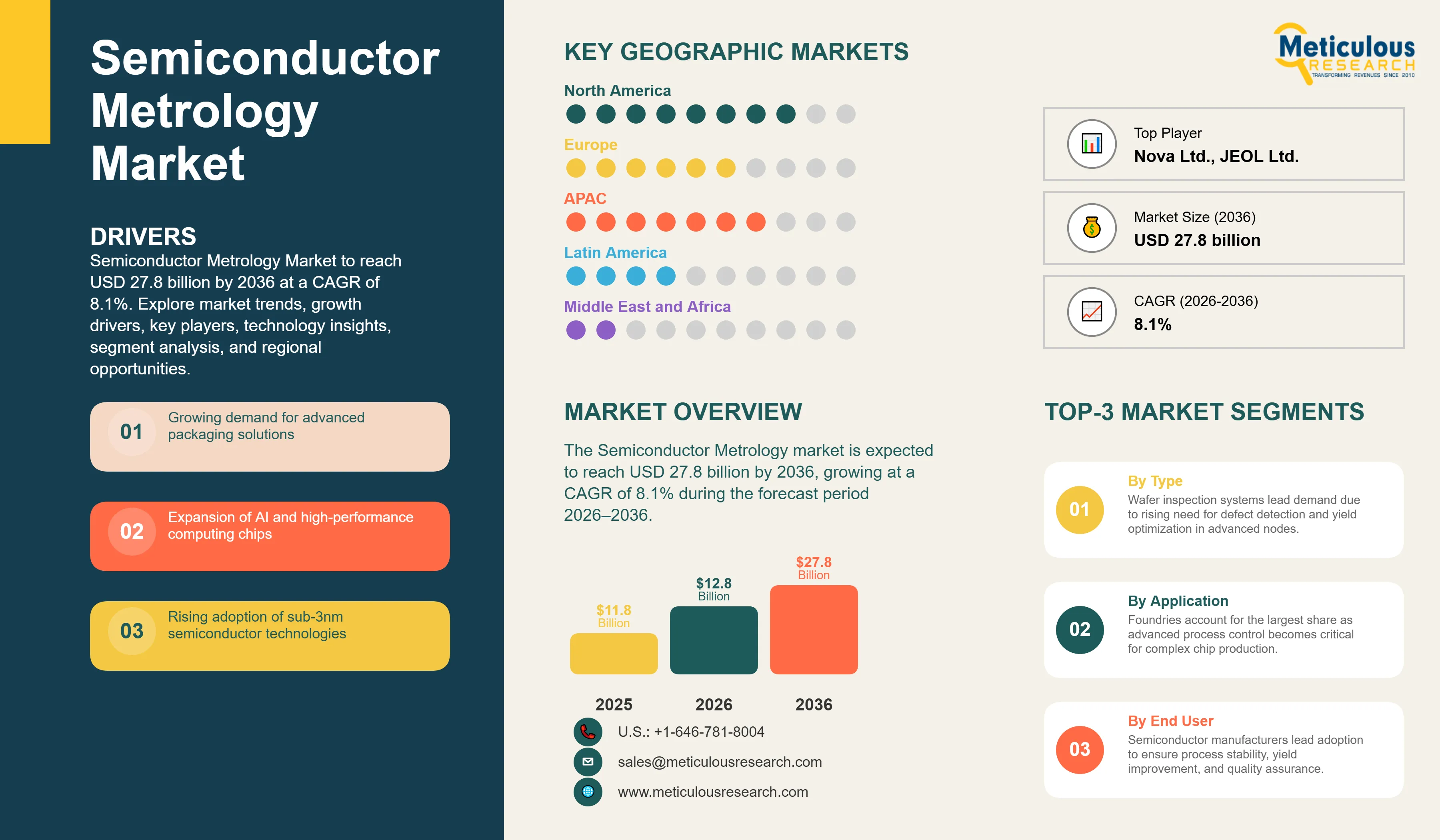
The global Semiconductor Metrology market is estimated to be USD 12.8 billion in 2026. This market is expected to reach USD 27.8 billion by 2036, growing at a CAGR of 8.1% during the forecast period 2026–2036.
Market Insights: Precision Measurement for the Semiconductor Frontier
 Click here to: Get Free Sample Pages of this Report
The global Semiconductor Metrology market is a critical enabler of the semiconductor industry's continued scaling, providing the precision measurement and inspection capabilities required to manufacture increasingly complex integrated circuits. As the industry advances toward sub-3 nm nodes and adopts new device architectures such as Gate-All-Around (GAA) transistors and advanced 3D NAND structures, demand for highly accurate, non-destructive metrology and inspection solutions is intensifying. Semiconductor metrology encompasses a range of technologies used to measure critical dimensions, analyze material characteristics, detect defects, and maintain process control throughout wafer fabrication and advanced packaging operations.
The market is being driven by robust investments in semiconductor manufacturing capacity worldwide. According to SEMI, global semiconductor fab capacity is projected to reach a record 33.7 million wafers per month (8-inch equivalent) in 2025, while leading-edge capacity below 5 nm is expected to expand by 17% in 2025 as manufacturers ramp production of GAA-based devices. SEMI further forecasts that advanced-node capacity (7 nm and below) will increase by approximately 69% between 2024 and 2028, reaching 1.4 million wafers per month, highlighting the growing need for sophisticated process control and metrology solutions. These investments are supported by the rapid proliferation of AI processors and high-performance computing applications, which require tighter process tolerances and higher yield performance.
Technology transitions are also increasing metrology complexity. TSMC commenced volume production of its 2 nm process in late 2025, marking its first commercial deployment of GAA nanosheet transistors. Such architectures require substantially more stringent critical dimension and overlay measurements compared with previous FinFET generations. Simultaneously, the emergence of High-NA EUV lithography is raising requirements for overlay accuracy and defect inspection. As semiconductor manufacturers pursue higher transistor densities and heterogeneous integration, advanced optical, electron-beam, and X-ray metrology systems are becoming indispensable for maintaining yield and ensuring process stability.
Moreover, the growing adoption of advanced packaging technologies, including chiplet architectures and wafer-level integration, is expanding the need for inspection and metrology beyond the front-end wafer fabrication stage. These trends are reinforcing the strategic importance of semiconductor metrology equipment, positioning the market as a fundamental component of the global semiconductor manufacturing ecosystem.
A primary driver for the semiconductor metrology market is the continuous push towards smaller process nodes, with the industry rapidly transitioning to sub-3nm technologies. This shrinkage necessitates metrology tools capable of measuring critical dimensions with atomic-level precision and detecting minute defects that can impact yield. As pitch sizes get smaller, inspection speed slows while accuracy demands increase, making advanced metrology indispensable. The adoption of novel transistor architectures like Gate-All-Around (GAA) and the increasing complexity of 3D NAND structures further drive the need for sophisticated metrology solutions. Additionally, the burgeoning advanced packaging market, which includes technologies like 2.5D and 3D stacking, requires new metrology techniques for wafer-to-wafer bonding, die-to-wafer stacking, and through-silicon via (TSV) inspection. The global semiconductor industry posted its highest-ever annual sales in 2025, nearly hitting $800 billion, with continued growth expected in 2026, directly fueling investments in manufacturing and, consequently, metrology equipment.
Despite robust growth drivers, the semiconductor metrology market faces significant restraints. The high capital expenditure associated with advanced metrology equipment poses a barrier, particularly for smaller foundries or those with limited R&D budgets. These tools often cost millions of dollars and require specialized cleanroom environments. The technical complexity of developing and operating these instruments is another challenge; as measurement requirements become more stringent, the R&D cycles lengthen, and the expertise required for tool development and maintenance increases. Furthermore, a persistent shortage of skilled engineers and technicians capable of operating and interpreting data from advanced metrology systems remains a critical restraint, impacting both equipment utilization and the pace of technological adoption.
Significant opportunities for growth in the semiconductor metrology market are emerging from the integration of Artificial Intelligence (AI) and machine learning (ML) for enhanced defect detection and process control. AI-driven metrology can accelerate data analysis, predict potential yield issues, and optimize inspection routines, leading to faster time-to-market and improved manufacturing efficiency. The increasing demand for in-situ and in-line metrology, which allows for real-time process monitoring without removing wafers from the production line, presents another substantial opportunity. This reduces cycle times and improves process feedback loops. Moreover, the development of new materials for advanced semiconductor devices (e.g., 2D materials, ferroelectrics) creates opportunities for novel material characterization techniques and specialized metrology tools, particularly in areas like polymer-based 'soft' materials for advanced packaging.
Integration of AI/ML for Enhanced Defect Detection and Process Control
A major trend in the semiconductor metrology market is the integration of AI and machine learning into defect inspection and process control workflows. AI-enabled metrology systems improve defect classification accuracy, optimize process parameters, and support predictive maintenance by analyzing the enormous volumes of data generated during wafer fabrication. According to SEMI, semiconductor manufacturers are rapidly adopting smart manufacturing practices as global wafer fab capacity is projected to reach 33.7 million wafers per month (8-inch equivalent) in 2025, increasing the amount of process data requiring automated analysis. In parallel, the International Energy Agency (IEA) estimates that demand for AI accelerators and data-center chips will continue to expand strongly through the decade, intensifying the need for higher yields and more sophisticated process control. As device architectures become increasingly complex, AI-driven metrology is emerging as a key tool for improving manufacturing efficiency and reducing defect-related losses.
Shift Towards In-Situ and In-Line Metrology
The industry is witnessing a transition from off-line, batch-based inspection toward in-situ and in-line metrology systems that provide real-time monitoring and feedback. This shift is driven by increasingly stringent process requirements at advanced nodes. SEMI forecasts that leading-edge capacity below 5 nm will expand by approximately 17% in 2025, while advanced-node capacity (7 nm and below) is expected to increase by nearly 69% between 2024 and 2028. Such scaling requires tighter overlay and critical-dimension control, making continuous process monitoring essential for minimizing wafer scrap and reducing cycle times. Consequently, semiconductor manufacturers are increasingly deploying integrated metrology solutions directly within production environments to enhance yield and throughput.
Growing Importance of 3D Metrology for Advanced Packaging
The rapid adoption of advanced packaging technologies, including 2.5D, 3D ICs, and chiplet-based architectures, is accelerating demand for high-precision 3D metrology solutions. According to SEMI, the advanced packaging market is expected to exceed USD 80 billion by 2028, supported by growing demand for AI processors and high-performance computing devices. In addition, the U.S. Department of Commerce's CHIPS Program highlights advanced packaging as a strategic priority for strengthening semiconductor supply chains and next-generation electronics manufacturing. These packaging approaches involve complex stacked structures and high-density interconnects that require non-destructive three-dimensional measurement and inspection capabilities. As a result, optical, X-ray, and electron-beam-based 3D metrology technologies are becoming increasingly critical for ensuring package quality, reliability, and yield.
Analysis by Type
Based on type, the wafer inspection systems segment is expected to hold the largest share in 2026. These systems are crucial for detecting defects and contaminants on the wafer surface at various stages of fabrication, directly impacting yield. The increasing complexity of chip designs and the shrinking feature sizes necessitate highly sensitive and high-throughput wafer inspection. The metrology equipment segment, encompassing tools for critical dimension (CD) measurement, overlay, and film thickness, is also a significant contributor. Mask inspection systems, essential for ensuring the quality of photomasks used in lithography, represent another vital segment.
Analysis by Technology
By technology, optical metrology is expected to account for the largest share in 2026. Its non-destructive nature, high resolution, and ability to perform various measurements (e.g., CD, overlay, film thickness) make it indispensable. Electron beam (e-beam) metrology, offering even higher resolution, is critical for advanced nodes and defect review. X-ray metrology is gaining traction for advanced packaging applications, particularly for measuring buried features and material composition. Other technologies, including atomic force microscopy (AFM) and scanning probe microscopy (SPM), provide ultra-high resolution for research and development.
Analysis by Application
By application, the foundry segment is expected to account for the largest share in 2026. Foundries, which manufacture chips for a wide range of fabless semiconductor companies, require extensive metrology capabilities to ensure process control and yield for diverse customer designs. IDMs (Integrated Device Manufacturers) also represent a significant application, as they manage both design and manufacturing. The OSAT (Outsourced Semiconductor Assembly and Test) segment is growing rapidly due to the increasing complexity of advanced packaging, driving demand for specialized metrology and inspection tools for assembly and test processes.
Analysis by End User
By end user, semiconductor manufacturers are expected to hold the largest share in 2026, as they are the direct consumers of metrology equipment for their fabrication facilities. Research and development (R&D) institutions, including universities and government labs, also represent a crucial end-user segment, driving innovation in new metrology techniques and tools. Material suppliers, who provide wafers and other raw materials, utilize metrology for quality control and characterization of their products. Other end users include equipment manufacturers and third-party testing services.
North America
North America is expected to witness significant growth in the semiconductor metrology market, fueled by substantial investments under the CHIPS Act and the resurgence of domestic manufacturing. Companies like Intel and GlobalFoundries are expanding their fabrication capabilities, driving demand for advanced metrology tools. The region also boasts a robust ecosystem of metrology equipment developers and research institutions, including NIST, which plays a critical role in establishing measurement standards for the semiconductor industry.
Asia Pacific
Asia Pacific is expected to dominate the global semiconductor metrology market in 2026, primarily due to the concentration of major foundries (e.g., TSMC, Samsung, SMIC) and memory manufacturers (e.g., SK Hynix). Countries like Taiwan, South Korea, China, and Japan are at the forefront of semiconductor manufacturing, driving immense demand for metrology and inspection equipment to ensure high yields and process control in their advanced fabs. The region's continuous investment in new fab construction further solidifies its leading position.
Europe
Europe represents a strong market for semiconductor metrology, particularly driven by its leadership in lithography equipment (ASML) and specialized metrology solutions. The region's focus on automotive and industrial power semiconductors, along with significant R&D investments in advanced materials and quantum computing, fuels the demand for high-precision metrology. European research institutions and companies are actively contributing to the development of next-generation metrology technologies.
Latin America
Latin America represents an emerging market for semiconductor metrology, with gradual adoption driven by increasing investments in digital infrastructure and the growing demand for advanced computing solutions in various industries. While still in its nascent stages, the region is expected to see increased interest in metrology technology as local industries seek to improve efficiency and performance in areas like data centers and telecommunications. Government initiatives to promote technological development and attract foreign investment will play a crucial role in accelerating market growth.
Middle East & Africa
The Middle East & Africa region is expected to witness steady growth in the semiconductor metrology market, primarily driven by investments in data centers, smart city initiatives, and the development of local technology ecosystems. Countries like the UAE and Saudi Arabia are actively diversifying their economies and investing in advanced technologies, including AI. The increasing demand for AI and HPC solutions in various sectors will contribute to the adoption of metrology in this region.
Competitive Landscape: Innovation, Strategic Partnerships, and Market Consolidation
The competitive landscape of the global semiconductor metrology market is highly concentrated, dominated by a few key players with extensive R&D capabilities and intellectual property. Innovation in advanced optical, e-beam, and X-ray technologies is crucial for maintaining market leadership. Strategic partnerships between metrology equipment providers and chip manufacturers are common, ensuring that tools are developed in alignment with future process roadmaps. The market also sees continuous consolidation as companies seek to acquire specialized technologies and expand their product portfolios. KLA Corporation, for instance, maintains the highest gross margin in the sector at 61%, reflecting its strong market position in process control and metrology [5].
KLA Corporation, Applied Materials, ASML Holding, Hitachi High-Tech, Lam Research, Tokyo Electron, Onto Innovation, Nova Ltd., Lasertec, Nikon, Canon, JEOL, Bruker, Oxford Instruments, Thermo Fisher Scientific, Carl Zeiss AG, Park Systems, Camtek, SCREEN Holdings, Rigaku Corporation.
The market is projected to reach USD 27.8 billion by 2036, growing at a CAGR of 8.1% from 2026 to 2036.
The primary drivers include the continuous push towards smaller process nodes (sub-3nm), the adoption of novel architectures like GAA transistors, and the increasing complexity of advanced packaging, all necessitating higher precision and defect detection.
The wafer inspection systems segment is expected to hold the largest share in 2026 due to increasing demand for defect detection and process control in advanced nodes.
Key challenges include the need for metrology tools capable of measuring critical dimensions with atomic-level precision, detecting minute defects, and addressing the complexities of 3D structures and advanced materials.
Asia Pacific is expected to dominate the global Semiconductor Metrology market in 2026, primarily due to the concentration of major foundries and memory manufacturers in the region.
Advanced packaging technologies like 2.5D and 3D stacking require new metrology techniques for wafer-to-wafer bonding, die-to-wafer stacking, and through-silicon via (TSV) inspection, particularly for 'soft' materials.
Optical metrology is expected to account for the largest share in 2026 due to its non-destructive nature, high resolution, and versatility in various measurements.
Key opportunities include the integration of AI/ML for enhanced defect detection, the shift towards in-situ and in-line monitoring, and the development of tools for advanced material characterization.
Semiconductor manufacturers are expected to hold the largest share in 2026, as they are the direct consumers of metrology equipment for their fabrication facilities.
The top 3 manufacturers are KLA Corporation, Applied Materials, Inc., and ASML Holding N.V.
1. Market Definition & Scope
1.1. Market Definition
1.2. Market Ecosystem
1.3. Currency Considered
1.4. Key Stakeholders
2. Research Methodology
2.1. Research Approach
2.2. Data Collection and Validation
2.2.1. Secondary Research
2.2.2. Primary Research/KOL Interviews
2.3. Market Sizing and Forecast
2.3.1. Market Size Estimation Approach
2.3.1.1. Bottom-Up Approach
2.3.1.2. Top-Down Approach
2.3.2. Growth Forecast Approach
2.3.3. Assumptions for the Study
3. Executive Summary
3.1. Overview
3.2. Segmental Analysis
3.2.1. Market Analysis, by Type
3.2.2. Market Analysis, by Technology
3.2.3. Market Analysis, by Application
3.2.4. Market Analysis, by End User
3.2.5. Market Analysis, by Geography
3.3. Competitive Analysis
4. Market Insights
4.1. Overview
4.2. Factors Affecting Market Growth
4.2.1. Drivers
4.2.1.1. Navigating the Complexity of Sub-3nm Nodes and Advanced Packaging
4.2.1.2. Escalating Demand for Advanced Lithography (e.g., High-NA EUV)
4.2.1.3. Increasing Investments in New Fab Construction and Capacity Expansion
4.2.2. Restraints
4.2.2.1. High Capital Expenditure and R&D Costs for Advanced Metrology Tools
4.2.2.2. Technical Complexity and Integration Challenges
4.2.2.3. Shortage of Skilled Workforce in Metrology and Inspection
4.2.3. Opportunities
4.2.3.1. AI-Driven Metrology for Enhanced Defect Detection and Process Control
4.2.3.2. Shift Towards In-Situ and In-Line Metrology for Real-Time Monitoring
4.2.3.3. Advanced Material Characterization for Novel Semiconductor Devices
4.2.4. Challenges
4.2.4.1. Maintaining Measurement Accuracy at Atomic-Scale Dimensions
4.2.4.2. Managing Data Volume and Complexity from High-Throughput Tools
4.2.4.3. Rapid Obsolescence of Metrology Equipment with Node Transitions
4.2.5. Trends
4.2.5.1. Integration of AI/ML for Enhanced Defect Detection and Process Control
4.2.5.2. Shift Towards In-Situ and In-Line Metrology
4.2.5.3. Growing Importance of 3D Metrology for Advanced Packaging
4.3. Porter’s Five Forces Analysis
4.4. Regulatory Landscape
4.5. Value Chain Analysis
5. Global Semiconductor Metrology Market, by Type
5.1. Overview
5.2. Wafer Inspection Systems
5.3. Metrology Equipment (CD, Overlay, Film Thickness)
5.4. Mask Inspection Systems
5.5. Other Types
6. Global Semiconductor Metrology Market, by Technology
6.1. Overview
6.2. Optical Metrology
6.3. Electron Beam (e-beam) Metrology
6.4. X-ray Metrology
6.5. Other Technologies
7. Global Semiconductor Metrology Market, by Application
7.1. Overview
7.2. Foundry
7.3. IDM (Integrated Device Manufacturer)
7.4. OSAT (Outsourced Semiconductor Assembly and Test)
7.5. Other Applications
8. Global Semiconductor Metrology Market, by End User
8.1. Overview
8.2. Semiconductor Manufacturers
8.3. Research & Development (R&D) Institutions
8.4. Material Suppliers
8.5. Other End Users
9. Global Semiconductor Metrology Market, by Geography
9.1. Overview
9.2. North America
9.2.1. U.S.
9.2.2. Canada
9.3. Europe
9.3.1. Germany
9.3.2. U.K.
9.3.3. France
9.3.4. Rest of Europe
9.4. Asia Pacific
9.4.1. China
9.4.2. Japan
9.4.3. South Korea
9.4.4. Taiwan
9.4.5. Rest of Asia Pacific
9.5. Latin America
9.5.1. Brazil
9.5.2. Mexico
9.5.3. Rest of Latin America
9.6. Middle East & Africa
9.6.1. UAE
9.6.2. Saudi Arabia
9.6.3. Rest of Middle East & Africa
10. Competitive Landscape
10.1. Introduction
10.2. Key Strategic Developments
10.3. Market Share Analysis
11. Company Profiles
11.1. KLA Corporation (U.S.)
11.2. Applied Materials, Inc. (U.S.)
11.3. ASML Holding N.V. (Netherlands)
11.4. Hitachi High-Tech Corporation (Japan)
11.5. Lam Research Corporation (U.S.)
11.6. Tokyo Electron Limited (Japan)
11.7. Onto Innovation Inc. (U.S.)
11.8. Nova Ltd. (Israel)
11.9. Lasertec Corporation (Japan)
11.10. Nikon Corporation (Japan)
11.11. Canon Inc. (Japan)
11.12. JEOL Ltd. (Japan)
11.13. Bruker Corporation (U.S.)
11.14. Oxford Instruments plc (U.K.)
11.15. Thermo Fisher Scientific Inc. (U.S.)
11.16. Carl Zeiss AG (Germany)
11.17. Park Systems Corp. (South Korea)
11.18. Camtek Ltd. (Israel)
11.19. SCREEN Holdings Co., Ltd. (Japan)
11.20. Rigaku Corporation (Japan)
12. Appendix
12.1. References
12.2. Disclaimer


Published Date: Feb-2026
Published Date: Feb-2026
Subscribe to get the latest industry updates