
Semiconductor Metrology Market (2026-2036)
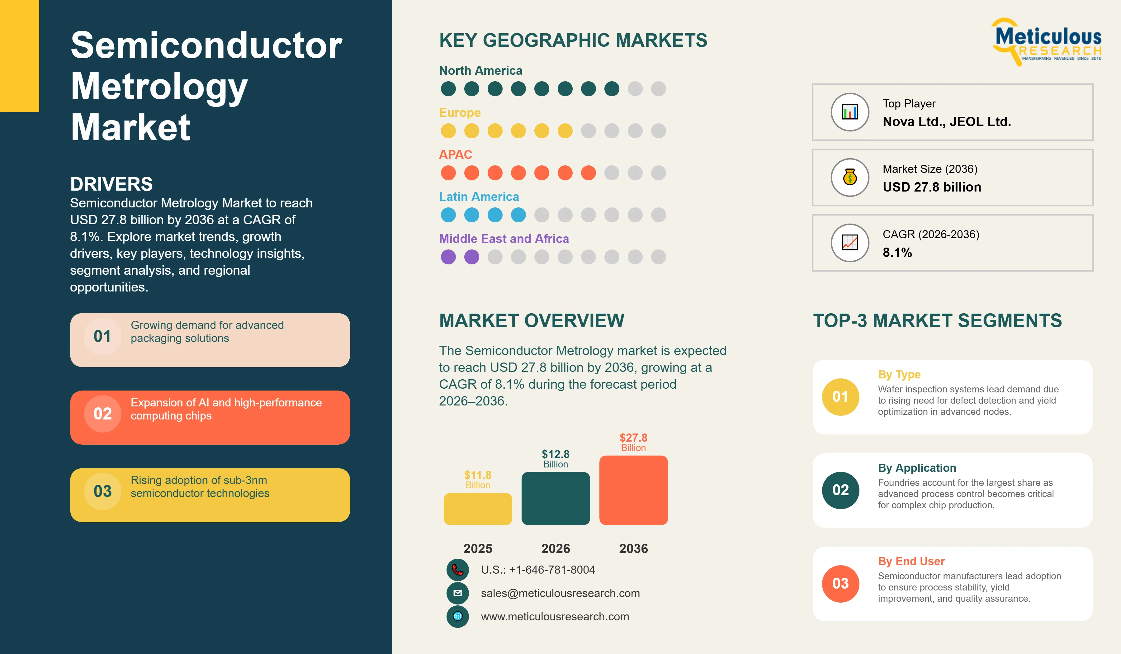
The global Semiconductor Metrology market is estimated to be USD 12.8 billion in 2026. This market is expected to reach USD 27.8 billion by 2036, growing at a CAGR of 8.1% during the forecast period 2026–2036.
- Published
- Jun 2026
- Pages
- 297
- Format
- PDF + Excel
- Report ID
- MRSE - 1042064
- Base year
- 2025
- 2026 · ESTIMATED
- $12.80B
- 2036
- $27.80B
- CAGR 2026–2036
- 8.1%
2025 baseline · 2026–2036 forecast at 8.1% CAGR · hover a bar for the value
Key highlights
The global Semiconductor Metrology market is projected to reach USD 27.8 billion by 2036, growing at a CAGR of 8.1% during the forecast period 2026–2036.
Asia Pacific is expected to dominate the global market in 2026, driven by the concentration of major foundries and memory manufacturers.
North America is projected to witness significant growth, fueled by CHIPS Act investments and the resurgence of domestic manufacturing.
By type, the wafer inspection systems segment is expected to hold the largest share in 2026, due to increasing demand for defect detection in advanced nodes.
By technology, optical metrology is expected to account for the largest share in 2026, driven by its non-destructive nature and high precision.
By application, the foundry segment is expected to account for the largest share in 2026, driven by the continuous demand for advanced process control.
Key players operating in the global market include KLA Corporation, Applied Materials, Inc., ASML Holding N.V., and Hitachi High-Tech Corporation.
Report summary
| Particulars | Details |
|---|---|
| Base Year | 2025 |
| Estimated Year | 2026 |
| Forecast Period | 2026–2036 |
| Market Size (2026) | USD 12.80 billion |
| Market Size (2036) | USD 27.80 billion |
| CAGR (2026–2036) | 8.1% |
| Format | PDF, Excel & Cloud Portal · 297 pages |
| Segments Covered | By Type · By Technology · By Application · By End User |
| Key Companies | KLA Corporation, Applied Materials, ASML Holding, Hitachi High-Tech, Lam Research, Tokyo Electron, Onto Innovation, Nova Ltd., Lasertec, Nikon, Canon, JEOL, Bruker, Oxford Instruments, Thermo Fisher Scientific, Carl Zeiss AG, Park Systems, Camtek, SCREEN Holdings, Rigaku Corporation |
Report infographic
Market dynamics
6 factors across 4 forcesNavigating the Complexity of Sub-3nm Nodes and Advanced Packaging
A primary driver for the semiconductor metrology market is the continuous push towards smaller process nodes, with the industry rapidly transitioning to sub-3nm technologies. This shrinkage necessitates metrology tools capable of measuring critical dimensions with atomic-level precision and detecting minute defects that can impact yield. As pitch sizes get smaller, inspection speed slows while accuracy demands increase, making advanced metrology indispensable. The adoption of novel transistor architectures like Gate-All-Around (GAA) and the increasing complexity of 3D NAND structures further drive the need for sophisticated metrology solutions. Additionally, the burgeoning advanced packaging market, which includes technologies like 2.5D and 3D stacking, requires new metrology techniques for wafer-to-wafer bonding, die-to-wafer stacking, and through-silicon via (TSV) inspection. The global semiconductor industry posted its highest-ever annual sales in 2025, nearly hitting $800 billion, with continued growth expected in 2026, directly fueling investments in manufacturing and, consequently, metrology equipment.
Table of contents
12 chapters · 115 sections · 297 pages · click to expandSegmental analysis
| Segment | Largest share (2026) | Fastest growth (2026–2036) |
|---|---|---|
| By Type | Wafer inspection systems | — |
| By Technology | Optical metrology | — |
| By Application | Foundry | — |
| By End User | Semiconductor manufacturers | — |
By Type
- The wafer inspection systems segment is expected to hold the largest share in 2026.
- These systems are crucial for detecting defects and contaminants on the wafer surface at various stages of fabrication, directly impacting yield.
- The increasing complexity of chip designs and the shrinking feature sizes necessitate highly sensitive and high-throughput wafer inspection.
- The metrology equipment segment, encompassing tools for critical dimension (CD) measurement, overlay, and film thickness, is also a significant contributor.
- Mask inspection systems, essential for ensuring the quality of photomasks used in lithography, represent another vital segment.
By Technology
- Optical metrology is expected to account for the largest share in 2026.
- Its non-destructive nature, high resolution, and ability to perform various measurements (e.g., CD, overlay, film thickness) make it indispensable.
- Electron beam (e-beam) metrology, offering even higher resolution, is critical for advanced nodes and defect review.
- X-ray metrology is gaining traction for advanced packaging applications, particularly for measuring buried features and material composition.
- Other technologies, including atomic force microscopy (AFM) and scanning probe microscopy (SPM), provide ultra-high resolution for research and development.
By Application
- The foundry segment is expected to account for the largest share in 2026.
- Foundries, which manufacture chips for a wide range of fabless semiconductor companies, require extensive metrology capabilities to ensure process control and yield for diverse customer designs.
- IDMs (Integrated Device Manufacturers) also represent a significant application, as they manage both design and manufacturing.
- The OSAT (Outsourced Semiconductor Assembly and Test) segment is growing rapidly due to the increasing complexity of advanced packaging, driving demand for specialized metrology and inspection tools for assembly and test processes.
By End User
- Semiconductor manufacturers are expected to hold the largest share in 2026, as they are the direct consumers of metrology equipment for their fabrication facilities.
- Research and development (R&D) institutions, including universities and government labs, also represent a crucial end-user segment, driving innovation in new metrology techniques and tools.
- Material suppliers, who provide wafers and other raw materials, utilize metrology for quality control and characterization of their products.
- Other end users include equipment manufacturers and third-party testing services.
Geographic analysis
North America
North America is expected to witness significant growth in the semiconductor metrology market, fueled by substantial investments under the CHIPS Act and the resurgence of domestic manufacturing. Companies like Intel and GlobalFoundries are expanding their fabrication capabilities, driving demand for advanced metrology tools. The region also boasts a robust ecosystem of metrology equipment developers and research institutions, including NIST, which plays a critical role in establishing measurement standards for the semiconductor industry. North America
Asia-Pacific
Largest shareAsia Pacific is expected to dominate the global semiconductor metrology market in 2026, primarily due to the concentration of major foundries (e.g., TSMC, Samsung, SMIC) and memory manufacturers (e.g., SK Hynix). Countries like Taiwan, South Korea, China, and Japan are at the forefront of semiconductor manufacturing, driving immense demand for metrology and inspection equipment to ensure high yields and process control in their advanced fabs. The region's continuous investment in new fab construction further solidifies its leading position. Asia Pacific
Europe
Europe represents a strong market for semiconductor metrology, particularly driven by its leadership in lithography equipment (ASML) and specialized metrology solutions. The region's focus on automotive and industrial power semiconductors, along with significant R&D investments in advanced materials and quantum computing, fuels the demand for high-precision metrology. European research institutions and companies are actively contributing to the development of next-generation metrology technologies. Europe
Latin America
Latin America represents an emerging market for semiconductor metrology, with gradual adoption driven by increasing investments in digital infrastructure and the growing demand for advanced computing solutions in various industries. While still in its nascent stages, the region is expected to see increased interest in metrology technology as local industries seek to improve efficiency and performance in areas like data centers and telecommunications. Government initiatives to promote technological development and attract foreign investment will play a crucial role in accelerating market growth. Latin America
Middle East & Africa
The Middle East & Africa region is expected to witness steady growth in the semiconductor metrology market, primarily driven by investments in data centers, smart city initiatives, and the development of local technology ecosystems. Countries like the UAE and Saudi Arabia are actively diversifying their economies and investing in advanced technologies, including AI. The increasing demand for AI and HPC solutions in various sectors will contribute to the adoption of metrology in this region. Middle East & Africa
Competitive landscape
The competitive landscape of the global semiconductor metrology market is highly concentrated, dominated by a few key players with extensive R&D capabilities and intellectual property. Innovation in advanced optical, e-beam, and X-ray technologies is crucial for maintaining market leadership. Strategic partnerships between metrology equipment providers and chip manufacturers are common, ensuring that tools are developed in alignment with future process roadmaps. The market also sees continuous consolidation as companies seek to acquire specialized technologies and expand their product portfolios. KLA Corporation, for instance, maintains the highest gross margin in the sector at 61%, reflecting its strong market position in process control and metrology [5].
- KLA Corporation
- Applied Materials
- ASML Holding
- Hitachi High-Tech
- Lam Research
- Tokyo Electron
- Onto Innovation
- Nova Ltd.
- Lasertec
- Nikon
- Canon
- JEOL
- Bruker
- Oxford Instruments
- Thermo Fisher Scientific
- Carl Zeiss AG
- Park Systems
- Camtek
- SCREEN Holdings
- Rigaku Corporation
Frequently asked questions
The market is projected to reach USD 27.8 billion by 2036, growing at a CAGR of 8.1% from 2026 to 2036.
Cite this report
Meticulous Research. (2026). Semiconductor Metrology Market - Global Opportunity Analysis and Industry Forecast (2026-2036) (Report No. MRSE - 1042064). Meticulous Market Research Pvt. Ltd. https://www.meticulousresearch.com/product/semiconductor-metrology-market-6747