Resources
About Us
Advanced Semiconductors Market Size, Share, & Forecast by Technology Node (2nm, 3nm, 5nm, 7nm), Product Type (Logic Chips, Memory Chips, Analog ICs, Processors), Application (AI/ML, 5G/6G, HPC, Automotive), End-Use Industry, and Packaging Technology - Global Forecasts (2026-2036)
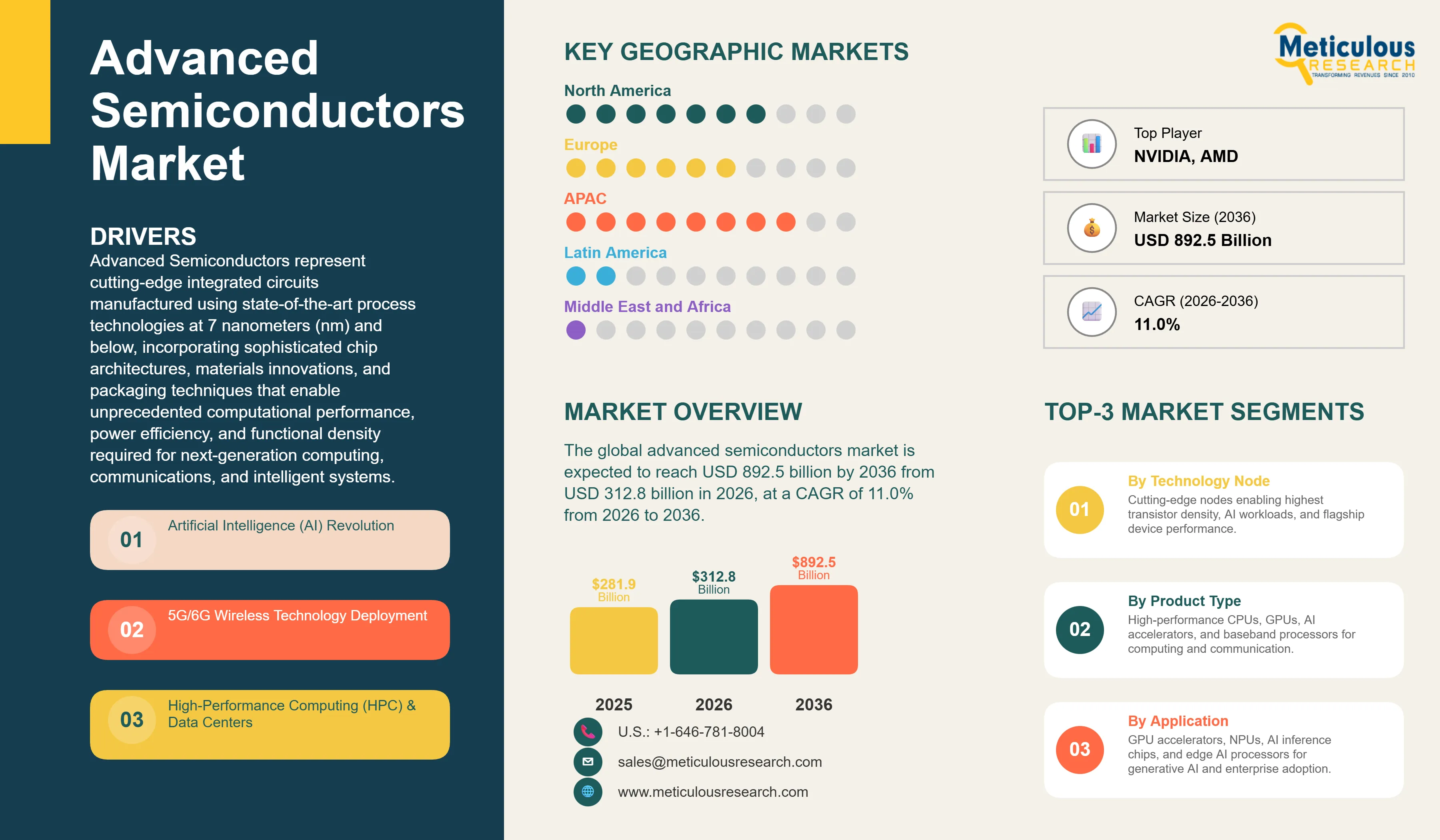
Report ID: MRSE - 1041715 Pages: 278 Feb-2026 Formats*: PDF Category: Semiconductor and Electronics Delivery: 24 to 72 Hours Download Free Sample ReportThe global advanced semiconductors market is expected to reach USD 892.5 billion by 2036 from USD 312.8 billion in 2026, at a CAGR of 11.0% from 2026 to 2036.
Advanced Semiconductors represent cutting-edge integrated circuits manufactured using state-of-the-art process technologies at 7 nanometers (nm) and below, incorporating sophisticated chip architectures, materials innovations, and packaging techniques that enable unprecedented computational performance, power efficiency, and functional density required for next-generation computing, communications, and intelligent systems. These semiconductor devices employ extreme ultraviolet (EUV) lithography enabling feature sizes approaching atomic scales, utilize novel materials including high-k metal gates, FinFET (fin field-effect transistor) and gate-all-around (GAA) transistor structures maximizing electrostatic control, integrate 3D stacking technologies and advanced packaging methods (chiplets, 2.5D/3D packaging) combining multiple dies for enhanced performance, implement specialized architectures optimized for artificial intelligence workloads (neural processing units, tensor cores), 5G/6G communications (RF transceivers, millimeter-wave components), and high-performance computing (multi-core processors, GPU accelerators), and achieve transistor densities exceeding 100-300 million transistors per square millimeter enabling complex system-on-chip (SoC) designs integrating CPU, GPU, memory, and specialized accelerators on single silicon die. By pushing the physical limits of semiconductor manufacturing through innovations in lithography, materials science, device physics, and chip architecture, advanced semiconductors enable transformative technologies including artificial intelligence capable of processing trillions of operations per second, 5G networks delivering multi-gigabit wireless speeds, autonomous vehicles processing sensor data in real-time, and hyperscale data centers supporting cloud computing and digital services, addressing the fundamental challenge that conventional semiconductor scaling approaches are reaching fundamental physical and economic limits requiring disruptive innovations in manufacturing processes, chip design methodologies, and system architectures.
 Click here to: Get Free Sample Pages of this Report
Advanced Semiconductors represent the technological frontier of the global electronics industry, enabling the computing power, energy efficiency, and functional capabilities required for artificial intelligence, 5G/6G communications, autonomous systems, and hyperscale cloud computing that define the digital economy. The semiconductor industry has followed Moore's Law—the observation that transistor density doubles approximately every two years—for over five decades, but advanced nodes below 7nm represent a fundamental inflection point where continued scaling requires revolutionary rather than evolutionary innovations in manufacturing processes, materials science, and chip architectures. The transition from planar transistors to FinFET structures at 22nm/16nm nodes, the adoption of extreme ultraviolet (EUV) lithography for 7nm and below, the development of gate-all-around (GAA) transistors for 3nm/2nm processes, and the integration of high-k metal gate materials demonstrate continuous innovation maintaining semiconductor performance improvements despite approaching atomic-scale dimensions where quantum effects, power consumption, and manufacturing complexity create formidable challenges.
Several transformative trends are reshaping the advanced semiconductors market, including the explosion of artificial intelligence driving unprecedented demand for specialized AI processors with massive parallel computing capabilities and high memory bandwidth, the proliferation of 5G networks requiring advanced RF transceivers and baseband processors handling gigabit data rates, the electrification and autonomization of automotive industry creating automotive-grade advanced semiconductor requirements, the geopolitical semiconductor competition with United States, China, European Union, Japan, and South Korea investing hundreds of billions in domestic semiconductor capabilities, the emergence of chiplet architectures and advanced packaging enabling continued performance scaling through heterogeneous integration when traditional process node shrinking faces diminishing returns, and the sustainability imperative driving power-efficient chip designs reducing data center energy consumption and extending mobile device battery life. The convergence of AI revolution—with ChatGPT demonstrating transformative potential and enterprises racing to deploy AI capabilities—mobile computing evolution toward 6G and edge intelligence, automotive transformation requiring processing power orders of magnitude beyond current vehicles, and geopolitical technology sovereignty concerns has elevated advanced semiconductors from enabling technology to strategic asset commanding hundreds of billions in government investments and representing critical economic and national security infrastructure.
The advanced semiconductors market is experiencing revolutionary transformation driven by artificial intelligence creating unprecedented demand for specialized processors optimized for machine learning workloads. AI applications require computational architectures fundamentally different from traditional CPUs—massive parallel processing executing thousands of operations simultaneously, high-bandwidth memory accessing vast datasets, tensor processing units optimized for matrix multiplication operations central to neural networks, and specialized accelerators for training large language models and running inference at scale. This drives explosive growth in GPU accelerators from NVIDIA dominating AI training with H100/B100 chips delivering exaFLOP-scale performance, custom AI processors including Google's TPUs, Amazon's Inferentia/Trainium, Microsoft's Maia, and Meta's MTIA designed for specific AI workloads, edge AI processors from Qualcomm, MediaTek, and others enabling on-device AI inference for smartphones and IoT, and neuromorphic chips exploring brain-inspired architectures for ultra-efficient AI processing. The generative AI revolution starting with ChatGPT has catalyzed massive AI infrastructure buildout—Microsoft, Google, Meta, and Amazon investing $200+ billion combined in AI data centers requiring millions of advanced AI chips—while enterprise AI adoption for automation, analytics, and augmentation creates sustained semiconductor demand across cloud providers and end-user organizations. AI processor requirements push leading-edge nodes: NVIDIA's H100 uses TSMC 4nm, next-generation B100 adopts TSMC 3nm, and future generations will leverage 2nm for maximum transistor density and power efficiency.
Extreme ultraviolet (EUV) lithography has emerged as enabling technology for advanced node manufacturing, overcoming fundamental limitations of conventional deep ultraviolet (DUV) lithography that required multiple patterning steps creating yield and cost challenges. EUV lithography uses 13.5nm wavelength light—versus 193nm for DUV—enabling single-exposure patterning of fine features that previously required 3-4 patterning steps, significantly improving manufacturing efficiency, yield, and design flexibility while enabling continued scaling to smaller nodes. ASML holds monopoly on EUV lithography systems with High-NA (numerical aperture) EUV machines costing $380+ million each achieving 8nm resolution for future 2nm and beyond nodes. The technology enables TSMC's 3nm process using 5-7 EUV layers, 2nm process targeting 10+ EUV layers, and future 1.4nm node potentially using exclusively EUV patterning. The EUV adoption creates significant barriers to entry: only TSMC, Samsung, and Intel possess EUV manufacturing capability with dozens of EUV scanners representing multi-billion dollar investments, while China's SMIC lacks EUV access due to export restrictions limiting advanced node capabilities. The technology roadmap includes next-generation High-NA EUV achieving higher resolution for sub-2nm nodes, although the escalating cost—a leading-edge fab now requires $15-20+ billion investment versus $3-5 billion for previous generations—concentrates advanced manufacturing among few players with financial resources and technical expertise.
Gate-all-around (GAA) transistor technology represents the next major transistor architecture evolution following FinFET, enabling continued electrostatic control and performance scaling at 3nm and beyond nodes. FinFET transistors used since 22nm/16nm nodes employ vertical fin structures surrounded by gate on three sides, but as dimensions shrink below 3nm, short-channel effects degrade transistor performance requiring new architectures. GAA transistors—implemented as nanosheets or nanowires with gate completely surrounding the channel—provide superior electrostatic control, reduced leakage current, better performance at lower voltages, and continued density scaling. Samsung introduced GAA (branded MBCFET) at 3nm node in 2022, TSMC is implementing GAA at 2nm node launching 2025, and Intel's RibbonFET represents their GAA implementation. The technology enables continued Moore's Law scaling: TSMC projects 2nm achieving 1.1-1.2x density improvement over 3nm, 15-20% performance gain or 25-30% power reduction, positioning 2nm for Apple A-series/M-series chips, flagship smartphone processors, and high-performance computing applications. However, GAA manufacturing introduces significant complexity including atomic layer deposition for gate stacks, precise nanosheet formation, and challenging integration with EUV lithography, contributing to escalating manufacturing costs and limiting GAA production to highest-value applications initially.
Advanced packaging technologies are emerging as critical enabler for continued semiconductor performance improvements as traditional 2D scaling approaches fundamental limits. Chiplet architectures disaggregate monolithic chips into smaller functional blocks (dies) that are heterogeneously integrated using advanced packaging, enabling mixing different process technologies (leading-edge logic with mature process memory), improving yields by producing smaller dies, accelerating development by reusing proven chiplets, and providing cost optimization using expensive advanced nodes only where performance-critical. Technologies including TSMC's CoWoS (Chip-on-Wafer-on-Substrate) 2.5D packaging used in NVIDIA H100 integrating GPU die with HBM memory achieving terabyte-per-second bandwidth, Intel's Foveros 3D stacking enabling vertical die integration, and AMD's chiplet approach in EPYC processors combining multiple compute dies demonstrate packaging's strategic importance. The shift toward chiplet architectures drives standardization efforts including UCIe (Universal Chiplet Interconnect Express) defining die-to-die interfaces enabling multi-vendor chiplet ecosystems, potentially transforming semiconductor industry from vertically integrated toward modular approaches where companies specialize in specific chiplet types. Advanced packaging also addresses power delivery and thermal challenges: as chips approach kilowatt-level power consumption, innovative cooling solutions including liquid cooling, and packaging innovations enabling efficient heat extraction become critical for maintaining performance and reliability.
The automotive semiconductor market is experiencing revolutionary transformation as vehicles evolve from mechanical systems with minimal electronics to software-defined platforms requiring advanced processing capabilities. Modern electric vehicles and autonomous driving systems demand computing power previously associated with data centers—Tesla's FSD (Full Self-Driving) computer processes camera, radar, and ultrasonic sensor data through dual neural processing units delivering 144 trillion operations per second, while next-generation autonomous platforms from companies including Mobileye, NVIDIA, and Qualcomm target even higher performance for Level 4/5 autonomy. This drives automotive adoption of advanced semiconductor nodes: automotive-grade 7nm/5nm processors from Qualcomm (Snapdragon Ride), NVIDIA (Orin/Thor), and others replace previous 28nm/40nm automotive chips, requiring extensive qualification for automotive reliability, temperature, and safety standards. The transformation extends beyond compute: power management ICs for battery systems, wide-bandgap semiconductors (SiC, GaN) for efficient power conversion, advanced sensors including LiDAR requiring specialized signal processing, and vehicle-to-everything (V2X) communication chips for 5G/6G connectivity. The automotive semiconductor content per vehicle is increasing from $600-800 in conventional vehicles to $1,500-2,000+ in electric vehicles and potentially $3,000+ in fully autonomous vehicles, creating massive market opportunity while challenging automotive supply chains traditionally designed for cost-optimized mature-process semiconductors to qualify and procure expensive leading-edge chips.
The artificial intelligence revolution is the primary market driver creating explosive demand for advanced semiconductors capable of training and running sophisticated AI models. The emergence of large language models (LLMs) including GPT-4, Claude, and Google's Gemini requiring thousands of GPUs for training, generative AI applications transforming content creation and software development, enterprise AI adoption for automation and analytics, and edge AI deployment for real-time inference in smartphones, IoT devices, and autonomous systems collectively drive unprecedented semiconductor demand. AI training workloads require massive parallel processing, high-bandwidth memory, and power-efficient architectures only achievable with leading-edge process technologies—NVIDIA's H100 Tensor Core GPU manufactured on TSMC 4nm delivers up to 4 petaFLOPS AI performance while consuming 700W, with next-generation B100 on 3nm targeting even higher performance density. The AI infrastructure buildout is massive: hyperscale cloud providers are projected to purchase 2-3 million AI accelerators annually 2024-2027 representing $100-150+ billion semiconductor spending, while enterprises deploying on-premises AI systems and edge AI devices create additional demand. The AI semiconductor market extends beyond training: inference acceleration for deploying AI models at scale, edge AI processors enabling on-device intelligence for privacy and latency, and specialized AI chips optimized for specific workloads (computer vision, natural language processing, recommendation systems) create diverse advanced semiconductor requirements across performance and power envelopes.
5G/6G wireless technology deployment is driving advanced RF and baseband semiconductor demand globally. 5G networks require fundamentally more sophisticated semiconductors than 4G LTE—supporting wider bandwidth (up to 100+ MHz channel widths versus 20MHz for LTE), higher frequencies including millimeter-wave bands (24-47 GHz) with different RF characteristics, massive MIMO antenna arrays requiring complex signal processing, and ultra-low latency for mission-critical applications—creating requirements only advanced process nodes can satisfy. Qualcomm's Snapdragon X75 5G modem manufactured on 4nm process, MediaTek's Dimensity 9300 integrating 5G in flagship SoC on 4nm, and Apple's custom 5G modems demonstrate smartphone 5G semiconductor complexity. The 5G infrastructure side drives demand for advanced baseband processors, RF front-end components, and network processors handling increased data throughput. Looking forward, 6G research targeting 2030 deployment anticipates even more demanding requirements including terahertz frequencies, AI-native network architectures, and integrated sensing and communication requiring next-generation advanced semiconductors. The wireless semiconductor market is global: 5G smartphone shipments exceeding 1 billion units annually create massive volume demand, while network infrastructure spanning base stations, small cells, and core network equipment drives additional advanced semiconductor consumption across diverse applications from smartphones to satellite communications.
High-performance computing (HPC) and data center infrastructure expansion is driving sustained advanced semiconductor demand. Modern data centers supporting cloud computing, streaming services, online gaming, social media, e-commerce, and enterprise applications require ever-increasing processing capacity—global data center IP traffic projected to grow from 20 zettabytes in 2023 to 50+ zettabytes by 2028 according to Cisco. This drives adoption of advanced server processors: AMD's EPYC using chiplet architecture on 5nm/4nm nodes capturing data center market share, Intel's Xeon Scalable processors transitioning to advanced nodes, and ARM-based server chips from Amazon (Graviton), Ampere, and others providing power-efficient alternatives. Data centers increasingly deploy specialized accelerators beyond CPUs—GPUs for graphics and AI, DPUs (data processing units) for networking and storage offload, FPGA accelerators for specific workloads, and custom ASICs including Google's TPUs—diversifying advanced semiconductor demand. The sustainability imperative amplifies advanced node importance: data centers consume 1-2% of global electricity with projections suggesting 8%+ by 2030 absent efficiency improvements. Advanced semiconductor nodes deliver 20-40% power reduction per generation enabling performance scaling while containing energy consumption and operational costs, making power efficiency critical data center procurement criterion driving adoption of latest process technologies for maximum performance-per-watt.
Geopolitical competition and technology sovereignty concerns are driving massive government investments in domestic advanced semiconductor capabilities. The United States CHIPS and Science Act allocates $52.7 billion for semiconductor manufacturing, R&D, and workforce development including $39 billion in manufacturing incentives driving Intel's $100+ billion U.S. fab expansion, TSMC's Arizona facilities targeting $65 billion investment with 3nm/2nm production planned, and Samsung's Texas expansion. The European Chips Act targets €43 billion investment doubling Europe's global semiconductor market share to 20% by 2030, supporting Intel's €30+ billion German fab complex and other European semiconductor projects. China's semiconductor self-sufficiency drive includes hundreds of billions in subsidies for domestic companies including SMIC, despite U.S. export restrictions limiting access to advanced manufacturing equipment. Japan and South Korea maintain semiconductor leadership through government-industry partnerships—Japan supporting Rapidus 2nm foundry development and Taiwan collaboration, South Korea providing tax incentives and infrastructure support for Samsung and SK Hynix expansions. These geopolitical dynamics recognize semiconductors as critical infrastructure underlying economic competitiveness, military capabilities, and technological leadership, creating unprecedented government support for advanced semiconductor development accelerating global capacity expansion and potentially reshaping geographic industry concentration from Asia-Pacific toward more distributed manufacturing footprint.
Escalating manufacturing costs and capital intensity pose fundamental challenge to advanced semiconductor industry sustainability. Leading-edge fab construction costs have increased exponentially—a state-of-the-art 2nm fab requires $20-25+ billion investment versus $15 billion for 3nm, $12 billion for 5nm, and $5 billion for 14nm facilities—while equipment costs spiral with individual High-NA EUV lithography systems costing $380+ million and complete fab requiring 50-100+ lithography tools plus thousands of other process equipment. The R&D costs similarly escalate: developing 2nm process technology requires multi-year effort, thousands of engineers, and $4-6+ billion investment in process development, design enablement, and manufacturing qualification. These economics limit leading-edge manufacturing to three players globally—TSMC, Samsung, and Intel—with financial resources and technical capabilities to sustain continuous process development, while GlobalFoundries, UMC, and other foundries have abandoned leading-edge competition focusing on mature process technologies where costs are manageable. The capital intensity creates strategic vulnerabilities: heavy depreciation burdens require high fab utilization rates and continuous technology transitions to justify investments, while cyclical demand fluctuations and potential overcapacity during downturns risk stranded assets. The industry faces sustainability question: whether escalating costs will force consolidation to single or two leading-edge manufacturers, whether alternative approaches including chiplets can reduce reliance on cutting-edge monolithic chips, or whether semiconductor economics must fundamentally restructure.
Talent shortage and workforce development challenges threaten advanced semiconductor industry growth as manufacturing reshores to new geographies and technical complexity increases. The semiconductor industry requires highly specialized workforce—process engineers understanding atomic-scale device physics and advanced materials, equipment engineers maintaining billion-dollar lithography and deposition systems, design engineers creating multi-billion transistor chips, and software engineers developing EDA tools and AI workloads—with expertise typically requiring advanced degrees and years of experience. The United States faces acute semiconductor workforce shortage: projected deficit of 67,000 technicians and engineers by 2030 according to industry estimates, while new CHIPS Act-funded fabs will require 50,000+ additional workers across construction, operations, and support. The challenge spans geographies: Europe, Japan, and other regions expanding semiconductor manufacturing face similar talent constraints, while even Taiwan and South Korea with mature semiconductor ecosystems compete for limited advanced expertise. Universities cannot rapidly scale specialized semiconductor programs, while competing technology sectors (software, AI, biotechnology) offer attractive alternatives for STEM graduates. The workforce challenge extends beyond quantity to quality: emerging technologies including GAA transistors, high-NA EUV lithography, and advanced packaging require expertise that doesn't exist broadly, necessitating extensive training programs and knowledge transfer. Companies address this through partnerships with universities, internal training programs, immigration of specialized talent, and automation reducing human workforce requirements, but talent constraints could limit pace of advanced semiconductor expansion despite government funding availability.
Technology Node Insights
The 3nm–5nm segment is expected to dominate the advanced semiconductor market in 2026 because it represents the most commercially viable leading-edge technology. These nodes deliver superior performance, higher transistor density, and lower power consumption compared to older generations, making them ideal for high-end applications. Major smartphone brands such as Apple, Samsung, and Google are adopting these nodes for flagship processors, while hyperscale cloud providers rely on them for AI accelerators and data center chips. Compared to 2nm and below, 3nm–5nm processes also offer better manufacturing yield and cost efficiency, making them more attractive for large-scale production. As a result, these nodes are likely to remain the industry workhorse for advanced computing, AI, and 5G infrastructure over the near term.
Product Insights:
Logic chips are expected to be the fastest-growing product category in the advanced semiconductor market due to surging demand from multiple high-growth industries. The rapid adoption of artificial intelligence is driving massive demand for GPUs, AI accelerators, and specialized processors used in training and deploying machine learning models. Data centers are scaling up investments in high-performance CPUs and custom silicon to handle increasing cloud workloads. Additionally, the global rollout of 5G networks is increasing demand for advanced baseband processors and networking chips. In the automotive sector, the transition toward electric vehicles and software-defined cars is creating new demand for powerful computing platforms that rely on advanced logic chips. Together, these trends are accelerating the shift toward smaller process nodes and higher-performance logic devices.
Application Insights
Based on application, the AI/ML segment is expected to dominate and experience the most rapid growth in 2026, driven by the global surge in artificial intelligence adoption across industries. This growth is largely powered by demand for high-performance computing components such as GPU accelerators, neural processing units (NPUs), specialized AI inference chips, and edge AI processors. The explosive rise of generative AI applications—such as large language models, image generation, and automated content creation—has significantly increased the need for advanced semiconductor solutions capable of handling massive data processing workloads. Enterprises across sectors including healthcare, finance, automotive, retail, and manufacturing are increasingly integrating AI into their operations for automation, predictive analytics, and decision-making, further boosting chip demand. Additionally, the shift toward edge AI—where data is processed locally on devices rather than in centralized cloud servers—is driving adoption of power-efficient, advanced-node processors for smartphones, IoT devices, robotics, and smart infrastructure. Together, these trends position AI/ML as the most influential application area shaping the advanced semiconductor market in 2026.
Regional Insights
In 2026, Asia-Pacific is estimated to account for the largest share of the global advanced semiconductor market due to its overwhelming manufacturing leadership and integrated electronics ecosystem. Taiwan’s TSMC remains the world’s most advanced foundry, producing chips at 3nm and below for major global tech companies, making it a critical pillar of the semiconductor supply chain. South Korea’s Samsung is another key leader in advanced logic and memory manufacturing, strengthening regional technological dominance. Meanwhile, China continues to invest massively in domestic semiconductor production to reduce dependency on foreign suppliers, supported by government subsidies, industrial policies, and strong end-market demand from consumer electronics, telecommunications, and electric vehicles. The region also hosts a dense network of semiconductor equipment suppliers, packaging firms, and electronics manufacturers, creating a highly concentrated and efficient value chain that reinforces Asia-Pacific’s leadership.
North America is projected to register significant growth in advanced semiconductors, primarily driven by the U.S. CHIPS and Science Act, which is stimulating large-scale investments in domestic chip fabrication plants by companies such as Intel, TSMC (Arizona), and Samsung (Texas). This policy shift aims to strengthen supply chain resilience, reduce geopolitical risks, and bring critical manufacturing back to the U.S. In parallel, North America maintains global leadership in fabless semiconductor design, with companies such as NVIDIA, AMD, Qualcomm, and Apple driving innovation in AI chips, data center processors, and mobile SoCs. The rapid expansion of cloud computing, artificial intelligence, autonomous vehicles, and defense electronics is further boosting demand for advanced nodes. Government strategic initiatives, public-private collaborations, and research funding in next-generation semiconductor technologies are expected to sustain long-term market momentum.
The advanced semiconductors market is expected to grow from USD 312.8 billion in 2026 to USD 892.5 billion by 2036.
The advanced semiconductors market is expected to grow at a CAGR of 11.0% from 2026 to 2036.
Major players include TSMC, Samsung, Intel, NVIDIA, AMD, Qualcomm, Apple, Broadcom, MediaTek, SK Hynix, Micron, ASML, Applied Materials, and Lam Research, among others.
Main factors include artificial intelligence revolution driving AI accelerator demand, 5G/6G deployment requiring advanced RF and baseband chips, data center expansion for cloud computing, automotive electrification and autonomy, geopolitical investments in semiconductor sovereignty (CHIPS Act), and continuous technology node advancement enabling performance scaling.
Asia-Pacific is estimated to account for the largest share in 2026 due to Taiwan's TSMC and South Korea's Samsung manufacturing dominance and regional electronics ecosystem, while North America is expected to register significant growth driven by CHIPS Act investments, fabless design leadership, and AI semiconductor innovation.
Key trends include transition to 2nm/3nm nodes with GAA transistors, EUV lithography advancement including High-NA EUV, chiplet architectures and advanced packaging (2.5D/3D), AI-specific processor designs, and integration of heterogeneous technologies through advanced packaging for continued performance scaling beyond traditional Moore's Law.


Published Date: Jun-2026
Published Date: Jan-2026
Published Date: Aug-2025
Published Date: Feb-2026
Please enter your corporate email id here to view sample report.
Subscribe to get the latest industry updates