Resources
About Us
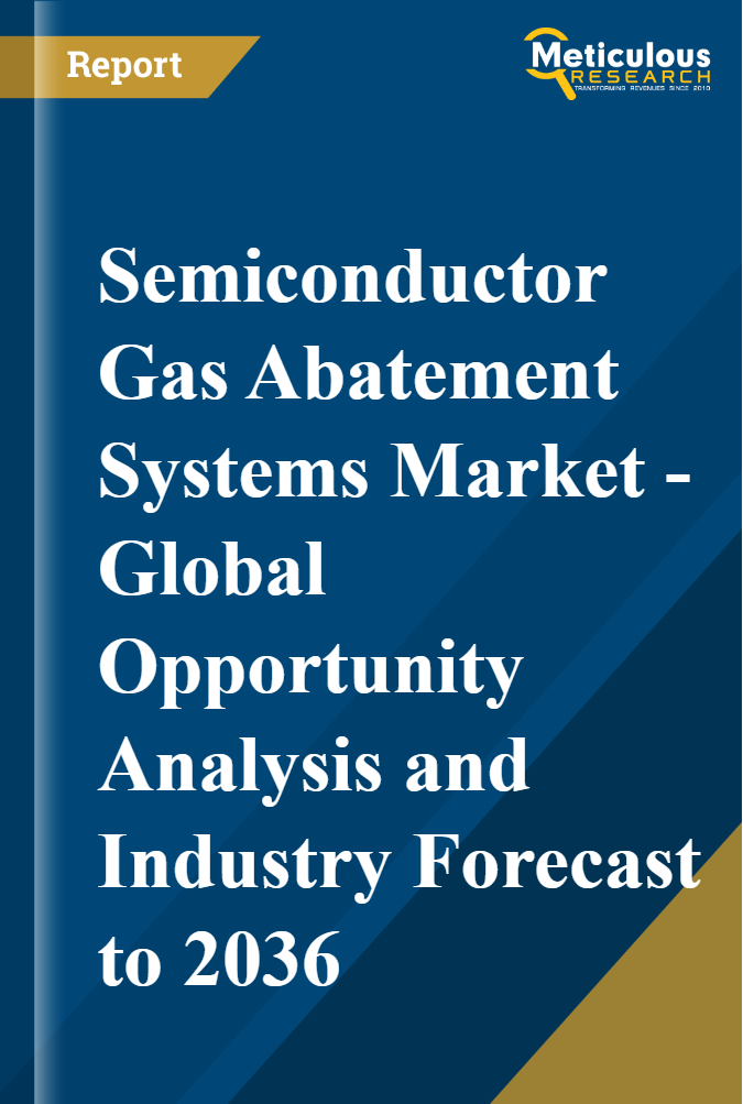
Semiconductor Gas Abatement Systems Market Size
The global Semiconductor Gas Abatement Systems Market was valued at USD 1.8 billion in 2025 and is projected to reach USD 1.9 billion in 2026. The market is expected to reach USD 4.3 billion by 2036, registering a CAGR of 8.4% during the forecast period (2026–2036).
Key Highlights
Market Overview
The Semiconductor Gas Abatement Systems Market comprises the equipment and technologies used to treat and neutralize hazardous, corrosive, and greenhouse process gases released during semiconductor fabrication steps such as etching, chemical vapor deposition, atomic layer deposition, and chamber cleaning. Abatement systems span point-of-use units installed directly at individual process tools, centralized systems that treat combined exhaust streams from multiple tools, and increasingly, integrated multi-stage systems that combine thermal, plasma, and wet treatment technologies to achieve high destruction and removal efficiency across complex gas mixtures.
Gas abatement is a mission-critical, non-discretionary element of semiconductor fab infrastructure, driven by both process necessity and environmental compliance. Semiconductor manufacturing uses a range of fluorinated process gases, including NF₃, CF₄, C₂F₆, CHF₃, and SF₆, in etching and chamber cleaning applications. According to the U.S. Environmental Protection Agency (EPA), semiconductor manufacturing uses high-global-warming-potential fluorinated compounds including PFCs, NF₃, and SF₆, and under normal operating conditions, approximately 10% to 80% of fluorinated greenhouse gases can pass through process chambers unreacted. The EPA reports 100-year global warming potentials of up to 11,100 for PFCs, 16,100 for NF₃, and 23,500 for SF₆, compared with CO₂'s reference value of 1, underscoring the importance of effective abatement technologies. These characteristics make high-efficiency abatement systems essential to semiconductor manufacturers' environmental compliance and sustainability commitments.
The market is benefiting from record levels of global semiconductor manufacturing investment. According to SEMI's latest 300mm Fab Outlook published in April 2026, worldwide 300mm fab equipment spending is projected to increase 18% to US$133 billion in 2026 and a further 14% to US$151 billion in 2027, surpassing US$150 billion for the first time. SEMI is tracking 413 fabs and production lines globally in its current 300mm outlook, while total installed 300mm capacity is projected to increase by approximately 7% in 2026. This sustained expansion of semiconductor manufacturing capacity is directly supporting demand for point-of-use and centralized gas abatement systems installed alongside etch, deposition, and cleaning equipment.
The AI-driven memory buildout provides an additional demand catalyst. SEMI projects 300mm memory fab equipment investment to reach US$52 billion in 2026, representing a 29% year-over-year increase, with DRAM equipment spending expected to reach US$37 billion and 3D NAND spending US$14 billion. The expansion of advanced DRAM, HBM, 3D NAND, and leading-edge logic production requires increasingly complex deposition and etching processes, increasing the number and complexity of process-gas streams that must be treated. Consequently, continued investment in AI semiconductor capacity is expected to translate into sustained demand for high-efficiency thermal, plasma, catalytic, and wet gas abatement systems.
Market Drivers
Expansion of Global Semiconductor Manufacturing Capacity
Sustained global investment in semiconductor manufacturing capacity, with SEMI projecting worldwide 300mm fab equipment spending to reach USD 133 billion in 2026 and USD 151 billion in 2027, is directly driving demand for gas abatement systems, as every new process tool installed in a fab requires an associated point-of-use or centralized abatement solution.
Increasing Construction of Advanced Semiconductor Fabs
Major semiconductor manufacturers are constructing new fabs across the United States, Taiwan, South Korea, Japan, and Europe to support both leading-edge and mature-node production, supported by regional policy incentives aimed at strengthening semiconductor supply chain resilience. Each new fab construction project requires comprehensive gas abatement infrastructure design and installation before production tools can be qualified for operation.
Market Restraints
High Capital and Operating Costs
Advanced gas abatement systems, particularly thermal and plasma-based technologies capable of achieving high destruction and removal efficiency for complex fluorinated gas mixtures, require substantial upfront capital investment as well as significant ongoing energy and consumables costs, representing a meaningful component of total fab operating expenditure.
Complex Process Gas Mixtures
Modern semiconductor fabs use an increasingly diverse range of process gases simultaneously across different tools and process steps, and abatement systems must be engineered to handle these complex, and sometimes reactive, gas mixtures reliably. Designing systems capable of treating multiple gas chemistries without compromising destruction efficiency remains a significant engineering challenge.
Market Opportunities
Growth of Advanced Node Semiconductor Manufacturing
The continued transition to sub-3nm process nodes is increasing the number of etch and deposition steps per wafer, each requiring dedicated gas abatement capacity. This trend is creating sustained demand for higher-performance abatement systems capable of meeting the increased throughput and efficiency requirements of leading-edge fabs.
Increasing Adoption of Low-GWP Process Gas Alternatives
Semiconductor manufacturers and gas suppliers are increasingly developing and adopting lower global-warming-potential alternatives to legacy PFC process gases. This transition is creating opportunities for abatement system suppliers to develop next-generation systems optimized for these new gas chemistries, supporting manufacturers' voluntary emission reduction commitments under World Semiconductor Council frameworks.
Market Trends
Growing Shift Toward Point-of-Use and Integrated Hybrid Abatement Systems
Fabs are increasingly deploying point-of-use abatement systems at individual process tools, and integrating multiple abatement technologies, such as combined thermal-plasma or plasma-wet hybrid systems, to achieve higher destruction efficiency across complex, multi-gas exhaust streams while optimizing energy consumption and footprint.
Rising Integration of Digital Monitoring and Predictive Maintenance
Semiconductor manufacturers are increasingly deploying real-time digital monitoring for gas concentration, emissions, and destruction and removal efficiency, combined with predictive maintenance analytics, to reduce the risk of compliance excursions and unplanned equipment downtime. This shift toward digitalized, condition-based abatement system management is expected to play a growing role across the industry.
Segment Analysis
Market Analysis by System Type
Based on system type, the global Semiconductor Gas Abatement Systems Market is segmented into Point-of-Use Gas Abatement Systems, Centralized Gas Abatement Systems, Integrated Abatement Systems, and Gas Abatement Monitoring & Control Systems.
In 2026, Point-of-Use Gas Abatement Systems are expected to account for the largest market share, reflecting fabs' growing preference for tool-specific abatement solutions that provide higher destruction efficiency and reduce cross-contamination risk. However, Integrated Abatement Systems are projected to register the fastest growth during the forecast period, driven by increasing adoption of multi-stage hybrid systems capable of treating complex, multi-gas exhaust streams from advanced-node process tools.
Market Analysis by Abatement Technology
Based on abatement technology, the market is segmented into Thermal Abatement, Plasma Abatement, Catalytic Abatement, Wet Scrubbing, Dry Abatement, and Hybrid Abatement.
In 2026, Thermal Abatement is expected to account for the largest market share, owing to its proven efficiency in handling high gas flow rates and meeting stringent emission regulations across a wide range of process gases. However, Plasma Abatement is projected to register the fastest growth, supported by its increasing adoption for high-efficiency destruction of fluorinated gases in advanced-node etch and deposition applications.
Market Analysis by Gas Type
Based on gas type, the market is segmented into Fluorinated Gases, Silane & Silicon-Containing Gases, Nitrogen-Containing Gases, Hydrogen & Hydrogen-Containing Gases, Oxygen-Containing Gases, and Other Hazardous Process Gases.
In 2026, Fluorinated Gases are expected to account for the largest market share, reflecting their widespread use in etching and chamber cleaning applications and the stringent abatement efficiency required given their high global warming potential. However, Silane & Silicon-Containing Gases are projected to register the fastest growth, driven by increasing use in deposition processes for advanced logic and memory device manufacturing.
Market Analysis by Semiconductor Process
Based on semiconductor process, the market is segmented into Etching, Chemical Vapor Deposition (CVD), Atomic Layer Deposition (ALD), Plasma-Enhanced CVD (PECVD), Cleaning Processes, Epitaxy, Ion Implantation, and Other Semiconductor Processes.
In 2026, Etching is expected to account for the largest market share, given its intensive use of fluorinated process gases requiring dedicated abatement capacity. However, Atomic Layer Deposition (ALD) is projected to register the fastest growth, driven by its expanding role in advanced-node gate and interconnect formation, which requires precise gas chemistry control and associated abatement infrastructure.
Market Analysis by Fab Type
Based on fab type, the market is segmented into Logic & Foundry Fabs, Memory Fabs (DRAM, NAND, and HBM), Analog & Power Semiconductor Fabs, Compound Semiconductor Fabs (Silicon Carbide and Gallium Nitride), MEMS & Sensor Fabs, and Advanced Packaging Facilities.
In 2026, Logic & Foundry Fabs are expected to account for the largest market share, consistent with SEMI's data identifying Logic & Micro, including Foundry, as the largest segment of global fab equipment spending. However, HBM Fabs, within the Memory Fabs segment, are projected to register the fastest growth, supported by surging demand for high-bandwidth memory used in AI accelerator chips.
Market Analysis by End User
Based on end user, the market is segmented into Semiconductor Foundries, Integrated Device Manufacturers (IDMs), Memory Manufacturers, Compound Semiconductor Manufacturers, MEMS & Sensor Manufacturers, Advanced Packaging & OSAT Providers, and Semiconductor Research & Development Facilities.
In 2026, Semiconductor Foundries are expected to account for the largest market share, reflecting the scale of new fab construction underway among leading contract manufacturers. However, Advanced Packaging & OSAT Providers are projected to register the highest CAGR, driven by rising process gas use in advanced packaging applications such as hybrid bonding and 3D packaging.
Geographic Analysis
Based on geography, the global Semiconductor Gas Abatement Systems Market is segmented into North America, Europe, Asia-Pacific, Latin America, and the Middle East & Africa.
In 2026, Asia-Pacific is expected to account for the largest share of the global Semiconductor Gas Abatement Systems Market. The region's leadership is supported by the concentration of semiconductor manufacturing capacity in Taiwan, South Korea, China, and Japan. According to SEMI's latest 300mm Fab Outlook, Taiwan, Korea, and China are expected to remain among the world's largest destinations for 300mm fab equipment investment, while global 300mm fab equipment spending is projected to reach US$133 billion in 2026. SEMI also projects that Taiwan's 300mm fab equipment investment will increase significantly through 2028, supported by continued expansion of leading-edge logic and advanced memory capacity. The expansion of 2nm and sub-2nm production in Taiwan is expected to require extensive new etching, deposition, and cleaning equipment and, consequently, additional point-of-use and centralized gas abatement infrastructure.
However, North America is projected to register the highest CAGR during the forecast period. The region's growth is driven by large-scale new fab construction supported by domestic semiconductor manufacturing incentives. According to SEMI's 2026 300mm Fab Outlook, the Americas are projected to account for approximately US$60 billion in 300mm fab equipment spending during 2026–2028, making the region one of the fastest-growing destinations for semiconductor manufacturing investment. SEMI is also tracking more than 400 global 300mm fabs and production lines, with additional capacity being added to support AI, advanced logic, memory, and automotive semiconductor demand. Every new etch, deposition, and chamber-cleaning process tool installed across these fab construction projects generates demand for appropriate gas treatment infrastructure, directly supporting regional demand for point-of-use thermal, plasma, catalytic, and wet abatement systems.
Competitive Landscape
The global Semiconductor Gas Abatement Systems Market is moderately consolidated, with competition among specialized gas abatement equipment manufacturers, industrial gas companies, and vacuum and exhaust system integrators. Companies compete primarily on destruction and removal efficiency performance, technology breadth across thermal, plasma, and wet abatement platforms, energy efficiency, and global service and support network coverage tied to major fab construction hubs.
Leading market participants are investing in developing higher-efficiency plasma and hybrid abatement technologies, expanding integrated monitoring and predictive maintenance capabilities, and forming strategic partnerships with semiconductor manufacturers and equipment OEMs to secure long-term system supply and service agreements tied to major new fab construction projects. Capacity expansions, technology upgrades, and energy-efficiency-focused product development remain key strategies adopted by major vendors.
The report provides a comprehensive competitive assessment of the leading companies operating in the global Semiconductor Gas Abatement Systems Market. The key players profiled in the report include Edwards Vacuum, Ebara Corporation, DAS Environmental Expert GmbH, Kanken Techno Co., Ltd., CS CLEAN SYSTEMS AG, Busch Vacuum Solutions, Ecosys Abatement, Plasma-Therm LLC, Linde plc, Air Liquide S.A., Fujifilm Holdings Corporation, MEKICS Co., Ltd., KNM Group Berhad, Kurita Water Industries Ltd., and Veolia Water Technologies.
Semiconductor Gas Abatement Systems Market Research Summary:
|
Particulars |
Details |
|
Forecast Period |
2026–2036 |
|
Base Year |
2025 |
|
Estimated Year |
2026 |
|
CAGR (Value) |
8.4% |
|
Market Size (Value) in 2026 |
USD 1.9 Billion |
|
Market Size (Value) in 2036 |
USD 4.3 Billion |
|
Segments Covered |
By System Type: Point-of-Use Gas Abatement Systems, Centralized Gas Abatement Systems, Integrated Abatement Systems, Gas Abatement Monitoring & Control Systems. By Abatement Technology: Thermal Abatement, Plasma Abatement, Catalytic Abatement, Wet Scrubbing, Dry Abatement, Hybrid Abatement. By Gas Type: Fluorinated Gases (NF₃, CF₄, C₂F₆, CHF₃, SF₆), Silane & Silicon-Containing Gases, Nitrogen-Containing Gases, Hydrogen & Hydrogen-Containing Gases, Oxygen-Containing Gases, Other Hazardous Process Gases. By Semiconductor Process: Etching, Chemical Vapor Deposition (CVD), Atomic Layer Deposition (ALD), Plasma-Enhanced CVD (PECVD), Cleaning Processes, Epitaxy, Ion Implantation, Other Semiconductor Processes. By Semiconductor Device: Logic Devices, Memory Devices (DRAM, NAND, HBM), Microprocessors & Microcontrollers, Analog & Mixed-Signal Devices, Power Semiconductors, RF & Connectivity Devices, Image Sensors, Compound Semiconductor Devices. By Fab Type: Logic & Foundry Fabs, Memory Fabs, Analog & Power Semiconductor Fabs, Compound Semiconductor Fabs, MEMS & Sensor Fabs, Advanced Packaging Facilities. By System Capacity: Small-Capacity Systems, Medium-Capacity Systems, Large-Capacity Systems, Multi-Tool/Multi-Chamber Systems. By End User: Semiconductor Foundries, Integrated Device Manufacturers (IDMs), Memory Manufacturers, Compound Semiconductor Manufacturers, MEMS & Sensor Manufacturers, Advanced Packaging & OSAT Providers, Semiconductor R&D Facilities. |
|
Countries Covered |
North America: U.S., Canada. Europe: Germany, France, U.K., Netherlands, Belgium, Ireland, Italy, Rest of Europe. Asia-Pacific: Taiwan, China, South Korea, Japan, Singapore, India, Malaysia, Vietnam, Rest of Asia-Pacific. Latin America: Brazil, Mexico, Argentina, Rest of Latin America. Middle East & Africa: Israel, UAE, Saudi Arabia, South Africa, Rest of Middle East & Africa. |
|
Key Companies |
Edwards Vacuum, Ebara Corporation, DAS Environmental Expert GmbH, Kanken Techno Co., Ltd., CS CLEAN SYSTEMS AG, Busch Vacuum Solutions, Ecosys Abatement, Plasma-Therm LLC, Linde plc, Air Liquide S.A., Fujifilm Holdings Corporation, MEKICS Co., Ltd., KNM Group Berhad, Kurita Water Industries Ltd., and Veolia Water Technologies. |
Key Questions Answered in the Report
The global Semiconductor Gas Abatement Systems Market is estimated at USD 1.9 billion in 2026.
The market is projected to reach USD 4.3 billion by 2036.
The market is driven by expanding global semiconductor manufacturing capacity, increasing construction of advanced fabs, growing use of specialty and process gases, increasing environmental regulations for semiconductor emissions, and growing adoption of point-of-use gas abatement systems.
Point-of-Use Gas Abatement Systems are expected to account for the largest market share in 2026.
Thermal Abatement is expected to account for the largest market share, owing to its proven efficiency in handling high gas flow rates.
Fluorinated Gases are expected to account for the largest market share, reflecting their widespread use in etching and chamber cleaning applications.
Logic & Foundry Fabs are expected to account for the largest market share, consistent with their position as the largest segment of global fab equipment spending.
Asia-Pacific is expected to remain the largest regional market, supported by the concentration of global semiconductor manufacturing capacity in Taiwan, South Korea, China, and Japan.
Leading companies include Edwards Vacuum, Ebara Corporation, DAS Environmental Expert, Kanken Techno, CS CLEAN SYSTEMS, Busch Vacuum Solutions, Ecosys Abatement, Plasma-Therm, Linde, Air Liquide, Fujifilm Holdings, MEKICS, KNM Group, Kurita Water Industries, and Veolia Water Technologies.
1. Introduction
1.1. Market Definition
1.2. Market Ecosystem
1.3. Currency and Limitations
1.3.1. Currency
1.3.2. Limitations
1.4. Key Stakeholders
2. Research Methodology
2.1. Research Approach
2.2. Data Collection & Validation Process
2.2.1. Secondary Research
2.2.2. Primary Research & Validation
2.2.2.1. Primary Interviews with Semiconductor & Gas Abatement Experts
2.2.2.2. Country-/Region-Level Analysis
2.3. Market Estimation
2.3.1. Bottom-Up Approach
2.3.2. Top-Down Approach
2.3.3. Forecast Methodology
2.4. Data Triangulation
2.5. Assumptions
3. Executive Summary
4. Market Overview
4.1. Introduction
4.2. Semiconductor Gas Abatement Process Overview
4.2.1. Process Gas Generation
4.2.2. Exhaust Gas Collection
4.2.3. Point-of-Use Abatement
4.2.4. Gas Treatment
4.2.5. Byproduct Removal
4.2.6. Exhaust Gas Monitoring
4.3. Market Dynamics
4.3.1. Drivers
4.3.1.1. Expansion of Global Semiconductor Manufacturing Capacity
4.3.1.2. Increasing Construction of Advanced Semiconductor Fabs
4.3.1.3. Growing Use of Specialty & Process Gases
4.3.1.4. Increasing Environmental Regulations for Semiconductor Emissions
4.3.1.5. Growing Adoption of Point-of-Use Gas Abatement Systems
4.3.2. Restraints
4.3.2.1. High Capital and Operating Costs
4.3.2.2. Complex Process Gas Mixtures
4.3.2.3. High Maintenance Requirements
4.3.2.4. Limited Availability of Skilled Technical Personnel
4.3.3. Opportunities
4.3.3.1. Growth of Advanced Node Semiconductor Manufacturing
4.3.3.2. Increasing Adoption of Low-GWP Process Gas Alternatives
4.3.3.3. Development of Energy-Efficient Abatement Systems
4.3.3.4. Increasing Demand for Integrated Gas Abatement & Monitoring
4.3.3.5. Expansion of Semiconductor Manufacturing in Emerging Regions
4.3.4. Challenges
4.3.4.1. Abatement of High-GWP Fluorinated Gases
4.3.4.2. Corrosive and Reactive Gas Byproducts
4.3.4.3. Maintaining High Destruction & Removal Efficiency
4.3.4.4. Managing Abatement Byproducts and Secondary Waste
4.4. Technology Landscape
4.4.1. Thermal Abatement
4.4.2. Plasma Abatement
4.4.3. Catalytic Abatement
4.4.4. Wet Abatement
4.4.5. Dry Abatement
4.4.6. Combustion-Based Abatement
4.4.7. Hybrid Abatement
4.4.8. Cryogenic & Condensation-Based Treatment
4.5. Semiconductor Gas Abatement Ecosystem
4.5.1. Specialty Gas Manufacturers
4.5.2. Semiconductor Equipment Manufacturers
4.5.3. Gas Abatement Equipment Manufacturers
4.5.4. Exhaust Treatment System Integrators
4.5.5. Semiconductor Foundries
4.5.6. Integrated Device Manufacturers (IDMs)
4.5.7. OSAT Providers
4.5.8. Environmental Technology Providers
4.6. Value Chain Analysis
4.6.1. Gas Generation & Supply
4.6.2. Semiconductor Process Equipment
4.6.3. Exhaust Gas Collection
4.6.4. Abatement Equipment Manufacturing
4.6.5. Installation & Integration
4.6.6. Operation & Maintenance
4.6.7. Byproduct & Waste Management
4.7. Regulatory & Environmental Landscape
4.7.1. EPA Regulations
4.7.2. European Emission Regulations
4.7.3. F-Gas Regulations
4.7.4. Semiconductor Environmental Standards
4.7.5. Local Air Emission Regulations
4.7.6. Greenhouse Gas Reporting Requirements
4.8. Porter's Five Forces Analysis
4.9. Investment & Industry Trends
4.9.1. Semiconductor Fab Construction
4.9.2. Advanced Node Manufacturing
4.9.3. Sustainable Semiconductor Manufacturing
4.9.4. Low-GWP Gas Adoption
4.9.5. Abatement System Energy Optimization
4.9.6. Digital Monitoring & Predictive Maintenance
4.10. Pricing & Cost Analysis
4.10.1. System Pricing by Abatement Technology
4.10.2. System Pricing by Capacity
4.10.3. Installation & Integration Costs
4.10.4. Energy Consumption Costs
4.10.5. Maintenance & Consumables Costs
4.10.6. Total Cost of Ownership
5. Semiconductor Gas Abatement Systems Market, by System Type (Primary Segmentation)
5.1. Introduction
5.2. Point-of-Use Gas Abatement Systems
5.2.1. Single-Tool Abatement Systems
5.2.2. Multi-Chamber Abatement Systems
5.2.3. Cluster Tool Abatement Systems
5.3. Centralized Gas Abatement Systems
5.3.1. Centralized Wet Scrubbers
5.3.2. Centralized Dry Scrubbers
5.3.3. Centralized Thermal Treatment Systems
5.3.4. Centralized Plasma Treatment Systems
5.4. Integrated Abatement Systems
5.4.1. Thermal-Plasma Systems
5.4.2. Thermal-Wet Systems
5.4.3. Plasma-Wet Systems
5.4.4. Multi-Stage Hybrid Systems
5.5. Gas Abatement Monitoring & Control Systems
5.5.1. Gas Concentration Monitoring
5.5.2. Emission Monitoring
5.5.3. Destruction & Removal Efficiency Monitoring
5.5.4. Automated Process Control
5.5.5. Predictive Maintenance & Analytics
6. Semiconductor Gas Abatement Systems Market, by Abatement Technology
6.1. Introduction
6.2. Thermal Abatement
6.2.1. Combustion-Based Systems
6.2.2. Electric Thermal Systems
6.2.3. Catalytic-Thermal Systems
6.3. Plasma Abatement
6.3.1. Microwave Plasma
6.3.2. RF Plasma
6.3.3. Arc Plasma
6.4. Catalytic Abatement
6.5. Wet Scrubbing
6.5.1. Packed-Bed Scrubbers
6.5.2. Venturi Scrubbers
6.5.3. Multi-Stage Scrubbers
6.6. Dry Abatement
6.7. Hybrid Abatement
7. Semiconductor Gas Abatement Systems Market, by Gas Type
7.1. Introduction
7.2. Fluorinated Gases
7.2.1. NF₃
7.2.2. CF₄
7.2.3. C₂F₆
7.2.4. CHF₃
7.2.5. SF₆
7.2.6. Other Fluorinated Gases
7.3. Silane & Silicon-Containing Gases
7.3.1. Silane (SiH₄)
7.3.2. Dichlorosilane (SiH₂Cl₂)
7.3.3. Trichlorosilane (SiHCl₃)
7.3.4. Other Silicon-Containing Gases
7.4. Nitrogen-Containing Gases
7.4.1. Ammonia (NH₃)
7.4.2. Nitrogen Oxides
7.4.3. Other Nitrogen-Containing Gases
7.5. Hydrogen & Hydrogen-Containing Gases
7.5.1. Hydrogen (H₂)
7.5.2. Hydrogen Chloride (HCl)
7.5.3. Hydrogen Bromide (HBr)
7.6. Oxygen-Containing Gases
7.6.1. Ozone
7.6.2. Oxygen
7.6.3. Other Oxygen-Containing Gases
7.7. Other Hazardous Process Gases
7.7.1. Chlorine
7.7.2. Boron-Containing Gases
7.7.3. Arsenic-Containing Gases
7.7.4. Phosphorus-Containing Gases
8. Semiconductor Gas Abatement Systems Market, by Semiconductor Process
8.1. Introduction
8.2. Etching
8.2.1. Dry Etching
8.2.2. Plasma Etching
8.2.3. Deep Reactive Ion Etching
8.3. Chemical Vapor Deposition (CVD)
8.4. Atomic Layer Deposition (ALD)
8.5. Plasma-Enhanced CVD (PECVD)
8.6. Cleaning Processes
8.6.1. Chamber Cleaning
8.6.2. Wafer Cleaning
8.7. Epitaxy
8.8. Ion Implantation
8.9. Other Semiconductor Processes
9. Semiconductor Gas Abatement Systems Market, by Semiconductor Device
9.1. Introduction
9.2. Logic Devices
9.3. Memory Devices
9.3.1. DRAM
9.3.2. NAND
9.3.3. HBM
9.4. Microprocessors & Microcontrollers
9.5. Analog & Mixed-Signal Devices
9.6. Power Semiconductors
9.7. RF & Connectivity Devices
9.8. Image Sensors
9.9. Compound Semiconductor Devices
10. Semiconductor Gas Abatement Systems Market, by Fab Type
10.1. Introduction
10.2. Logic & Foundry Fabs
10.3. Memory Fabs
10.3.1. DRAM Fabs
10.3.2. NAND Fabs
10.3.3. HBM Fabs
10.4. Analog & Power Semiconductor Fabs
10.5. Compound Semiconductor Fabs
10.5.1. Silicon Carbide Fabs
10.5.2. Gallium Nitride Fabs
10.6. MEMS & Sensor Fabs
10.7. Advanced Packaging Facilities
11. Semiconductor Gas Abatement Systems Market, by End User
11.1. Introduction
11.2. Semiconductor Foundries
11.3. Integrated Device Manufacturers (IDMs)
11.4. Memory Manufacturers
11.5. Compound Semiconductor Manufacturers
11.6. MEMS & Sensor Manufacturers
11.7. Advanced Packaging & OSAT Providers
11.8. Semiconductor Research & Development Facilities
12. Semiconductor Gas Abatement Systems Market, by System Capacity
12.1. Introduction
12.2. Small-Capacity Systems
12.3. Medium-Capacity Systems
12.4. Large-Capacity Systems
12.5. Multi-Tool/Multi-Chamber Systems
13. Semiconductor Gas Abatement Systems Market, by Geography
13.1. Introduction
13.2. North America
13.2.1. U.S.
13.2.2. Canada
13.3. Europe
13.3.1. Germany
13.3.2. France
13.3.3. U.K.
13.3.4. Netherlands
13.3.5. Belgium
13.3.6. Ireland
13.3.7. Italy
13.3.8. Rest of Europe
13.4. Asia-Pacific
13.4.1. Taiwan
13.4.2. China
13.4.3. South Korea
13.4.4. Japan
13.4.5. Singapore
13.4.6. India
13.4.7. Malaysia
13.4.8. Vietnam
13.4.9. Rest of Asia-Pacific
13.5. Latin America
13.5.1. Brazil
13.5.2. Mexico
13.5.3. Argentina
13.5.4. Rest of Latin America
13.6. Middle East & Africa
13.6.1. Israel
13.6.2. UAE
13.6.3. Saudi Arabia
13.6.4. South Africa
13.6.5. Rest of Middle East & Africa
14. Competitive Landscape
14.1. Overview
14.2. Key Growth Strategies
14.3. Competitive Benchmarking
14.4. Competitive Dashboard
14.4.1. Market Leaders
14.4.2. Market Differentiators
14.4.3. Vanguards
14.4.4. Emerging Players
14.5. Market Share/Rank Analysis, by Key Player (2025)
14.6. Strategic Developments
14.6.1. Product Launches
14.6.2. Capacity Expansions
14.6.3. Partnerships & Collaborations
14.6.4. Mergers & Acquisitions
14.6.5. Contracts & Agreements
15. Company Profiles
(Business Overview, Financial Overview, Semiconductor Gas Abatement Portfolio,
Technology Capabilities, Strategic Developments, SWOT Analysis)
15.1. Edwards Vacuum
15.2. Ebara Corporation
15.3. DAS Environmental Expert GmbH
15.4. Kanken Techno Co., Ltd.
15.5. CS CLEAN SYSTEMS AG
15.6. Busch Vacuum Solutions
15.7. Ecosys Abatement
15.8. Plasma-Therm LLC
15.9. Linde plc
15.10. Air Liquide S.A.
15.11. Fujifilm Holdings Corporation
15.12. MEKICS Co., Ltd.
15.13. KNM Group Berhad
15.14. Kurita Water Industries Ltd.
15.15. Veolia Water Technologies
16. Appendix
16.1. Related Reports
16.2. Customization Options



















Published Date: Aug-2026
Published Date: Jun-2026
Published Date: Feb-2026
Subscribe to get the latest industry updates