Advanced Semiconductor Packaging Materials Market
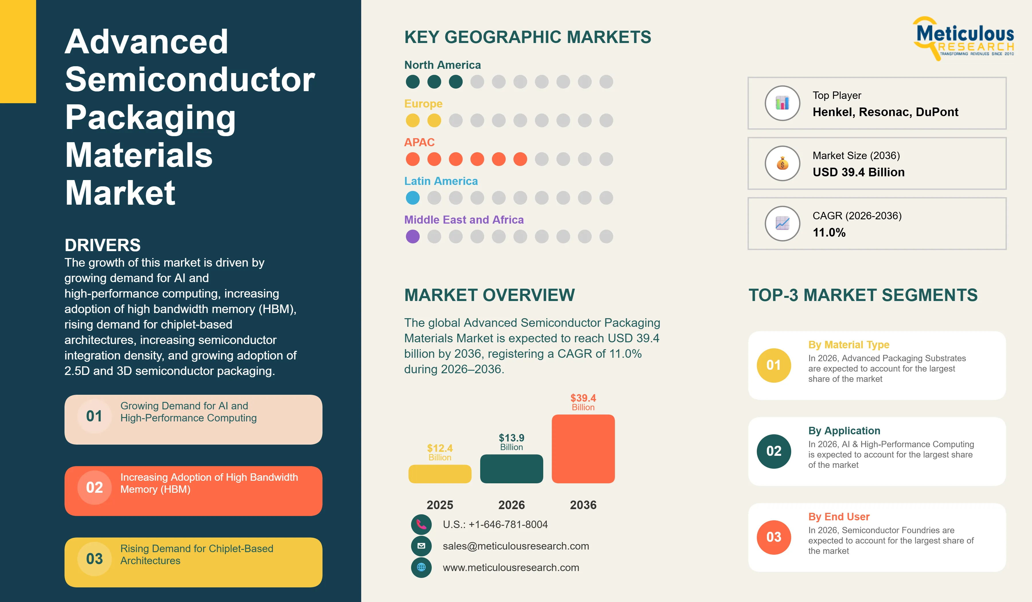
The global Advanced Semiconductor Packaging Materials Market was valued at USD 12.4 billion in 2025 and is projected to reach USD 13.9 billion in 2026. The market is expected to reach USD 39.4 billion by 2036, registering a CAGR of 11.0% during the forecast period (2026-2036).
- Published
- Aug 2026
- Pages
- 310
- Format
- PDF + Excel
- Report ID
- MR-2133
- Base year
- 2025
- 2024 · HISTORICAL
- $46.10B
- 2036
- $39.40B
- CAGR 2026–2036
- 11.0%
2024–2025 baseline · 2026–2036 forecast at 11.0% CAGR · hover a bar for the value
Key highlights
The global Advanced Semiconductor Packaging Materials Market is projected to reach USD 39.4 billion by 2036, driven by growing demand for AI and high-performance computing and increasing adoption of high bandwidth memory (HBM).
Asia-Pacific is expected to account for the largest market share in 2026, while North America is projected to register the fastest growth during the forecast period.
By material type, Advanced Packaging Substrates are expected to account for the largest market share, whereas Hybrid Bonding Dielectrics and Interconnect Materials are projected to witness the fastest growth through 2036.
By packaging technology, 2.5D Interposer-Based Packaging is expected to dominate the market, while Hybrid Bonding is projected to register the highest CAGR during the forecast period.
More than 78% of advanced semiconductor packages now use specialized thermal interface and substrate materials to manage electrical conductivity and heat dissipation, with over 64% of next-generation packages incorporating ceramic-based materials such as aluminum nitride and silicon carbide.
Intel and Samsung's 2026 pivot from organic to glass-core substrates, with Intel demonstrating a thick-core glass substrate combined with EMIB packaging at NEPCON Japan and SK Absolics targeting mass production in 2026, is expected to create significant long-term opportunities for advanced substrate material suppliers.
Report summary
| Particulars | Details |
|---|---|
| Forecast Period | 2026-2036 |
| Base Year | 2025 |
| Estimated Year | 2026 |
| CAGR (Value) | 11.0% |
| Format | PDF, Excel & Cloud Portal · 310 pages |
| Market Size (Value) in 2026 | USD 13.9 Billion |
| Market Size (Value) in 2036 | USD 39.4 Billion |
| Segments Covered | By Material Type: Advanced Packaging Substrates (Organic, Glass, Ceramic, Silicon), Interposer Materials (Silicon, Glass, Organic), Dielectric Materials (RDL, Build-Up, Low-Dk, Low-Df, Hybrid Bonding), Underfill Materials, Encapsulation & Molding Materials, Die Attach Materials, Interconnect Materials (Solder, Copper Pillars/Bumps, Hybrid Bonding Copper), Thermal Management Materials, Wafer-Level Processing Materials, Temporary Bonding & Debonding Materials. · By Packaging Technology: Flip-Chip Packaging, Fan-Out Wafer-Level Packaging, Fan-Out Panel-Level Packaging, 2.5D Interposer-Based Packaging, 3D IC Packaging, HBM Packaging, Chiplet-Based Packaging, System-in-Package (SiP), Hybrid Bonding, Heterogeneous Integration. · By Material Function: Electrical Interconnection, Dielectric Insulation, Mechanical Reinforcement, Thermal Management, Encapsulation & Protection, Stress & Warpage Management, Signal Integrity Management, Surface Protection. · By Application: AI & High-Performance Computing, High Bandwidth Memory, Advanced Logic & Computing, Mobile & Consumer Electronics, Automotive Electronics, Networking & Communications. By Semiconductor Device Type: Logic Devices, Memory Devices (HBM, DRAM, NAND), Microprocessors & Microcontrollers, AI Accelerators, Analog & Mixed-Signal Devices, Power Semiconductors, RF & Connectivity Devices, Image Sensors, Photonic & Optoelectronic Devices. · By End User: Semiconductor Foundries, IDMs, Memory Manufacturers, OSAT Providers, Advanced Packaging Specialists, Semiconductor R&D Organizations. |
| Countries Covered | North America: U.S., Canada. · Europe: Germany, France, U.K., Netherlands, Belgium, Italy, Rest of Europe. · Asia-Pacific: Taiwan, China, South Korea, Japan, Singapore, India, Malaysia, Vietnam, Rest of Asia-Pacific. · Latin America: Brazil, Mexico, Argentina, Rest of Latin America. · Middle East & Africa: Israel, UAE, Saudi Arabia, South Africa, Rest of Middle East & Africa. |
| Key Companies | Henkel AG & Co. KGaA, Resonac Holdings Corporation, Shin-Etsu Chemical Co., Ltd., DuPont de Nemours, Inc., Dow Inc., Samsung Electro-Mechanics Co., Ltd., Ajinomoto Co., Inc., NAMICS Corporation, Sumitomo Bakelite Co., Ltd., Kanto Chemical Co., Inc., Fujifilm Corporation, Merck KGaA, Indium Corporation, MacDermid Alpha Electronics Solutions, and ASE Technology Holding Co., Ltd. |
Report overview
Segments covered: material type, packaging technology, material function, application, end user, semiconductor device type.
The Advanced Semiconductor Packaging Materials Market comprises the specialized substrates, dielectrics, underfills, encapsulants, die attach compounds, interconnect materials, and thermal management materials used to build 2.5D, 3D, fan-out, chiplet-based, and hybrid-bonded semiconductor packages. These materials are engineered to meet increasingly stringent electrical, thermal, and mechanical performance requirements as packaging becomes the primary lever for performance gains in AI accelerators, high-performance computing, high-bandwidth memory, and advanced logic devices, given that traditional transistor scaling is approaching its physical limits.
Materials demand is closely tracking the industry's shift toward heterogeneous integration. Advanced packaging is becoming an increasingly important part of semiconductor performance scaling; industry estimates cited by SEMI project global advanced-packaging revenue to increase from US$46.1 billion in 2024 to US$79.4 billion by 2030. This expansion is increasing demand for high-performance substrates, dielectric materials, underfills, encapsulants, interconnect materials, and thermal-management solutions.
The growing intensity of AI and HBM applications is further increasing materials requirements per package. TSMC is expanding its CoWoS advanced-packaging platform to support larger interposers and greater integration of high-bandwidth memory, with the company completing certification of a 5.5-times mask/reticle-size CoWoS solution in 2025 and initiating volume production in 2026. As package sizes increase and chiplets, HBM stacks, and heterogeneous integration become more prevalent, requirements for thermal management, fine-pitch interconnects, low-loss dielectric materials, underfill reliability, and advanced substrates are intensifying. SEMI also forecasts semiconductor assembly and packaging equipment sales to reach US$6.7 billion in 2026, reflecting continued investment in advanced and heterogeneous packaging technologies for AI and HBM devices
The market is also being reshaped by a generational shift in substrate materials. In a pivot described by industry analysts as the most significant packaging material change in decades, Intel and Samsung began transitioning from organic resin substrates toward glass-core substrates in early 2026 to meet the thermal and interconnect demands of generative AI packages, with Intel demonstrating a thick-core glass substrate combined with EMIB packaging at NEPCON Japan in January 2026 and SK Absolics targeting mass production later that year.
Report infographic
Market dynamics
8 factors across 4 forcesGrowing Demand for AI and High-Performance Computing
The rapid expansion of AI accelerator, GPU, and high-performance computing chip production is a primary driver of demand for advanced packaging materials, as these devices increasingly rely on 2.5D and 3D packaging architectures that require specialized substrates, dielectrics, interconnects, underfills, and thermal management materials. According to SEMI, global 300mm fab equipment spending is expected to reach approximately US$142 billion in 2026, representing a 25% year-over-year increase, with AI and high-performance computing applications among the key drivers of capacity expansion. The demand for high-bandwidth memory (HBM), which is increasingly integrated with AI accelerators through advanced 2.5D packaging, is also driving substantial investment; SEMI projects 300mm memory fab equipment investment to exceed US$50 billion in 2026. As AI accelerator packages become increasingly larger and integrate multiple chiplets and HBM stacks, TSMC's CoWoS technology has progressed toward packages using interposers up to 5.5 times the size of the maximum reticle, with volume production of this large-format solution beginning in 2026. These trends are increasing requirements for low-loss substrates, advanced dielectrics, high-performance interconnect materials, underfills, and thermal management solutions while driving innovation toward higher-value advanced packaging materials.
Increasing Adoption of High Bandwidth Memory (HBM)
The rapid scaling of HBM capacity to support AI accelerator platforms is driving significant demand for specialized interposer materials, hybrid bonding dielectrics, and thermal management materials. As HBM manufacturers transition through HBM3E toward HBM4 and HBM5 generations with rising stack counts, the associated packaging materials must meet increasingly stringent thermal conductivity and fine-pitch interconnect requirements.
Table of contents
8 chapters · 280 sections · 310 pages · click to expandSegmental analysis
| Segment | Largest share (2026) | Fastest growth (2026–2036) |
|---|---|---|
| By Material Type | Advanced Packaging Substrates | Interconnect Materials |
| By Packaging Technology | 2.5D Interposer-Based Packaging | Hybrid Bonding |
| By Application | AI & High-Performance Computing | High Bandwidth Memory |
| By End User | Semiconductor Foundries | Memory Manufacturers |
By Material Type
- Advanced Packaging Substrates are expected to account for the largest market share, reflecting their foundational role across nearly all advanced package architectures and the accelerating transition from organic to glass substrate materials.
- However, Interconnect Materials, particularly hybrid bonding copper materials, are projected to register the fastest growth during the forecast period, driven by rapid hybrid bonding adoption across HBM and advanced logic applications.
By Packaging Technology
- 2.5D Interposer-Based Packaging is expected to account for the largest market share, supported by its widespread use in AI accelerator and HBM packaging platforms such as TSMC's CoWoS.
- However, Hybrid Bonding is projected to register the highest CAGR during the forecast period, driven by its accelerating adoption across HBM, advanced logic, and image sensor applications.
By Application
- AI & High-Performance Computing is expected to account for the largest market share, reflecting the outsized role AI GPUs, AI accelerators, and custom AI ASICs play in driving advanced packaging materials demand.
- However, High Bandwidth Memory is projected to register the highest CAGR during the forecast period, as HBM manufacturers scale capacity through successive HBM4 and HBM5 generations.
By End User
- Semiconductor Foundries are expected to account for the largest market share, led by leading-edge players expanding advanced packaging capacity to serve AI and HPC customers.
- However, Memory Manufacturers are projected to register the highest CAGR during the forecast period, as HBM producers scale materials consumption across successive generations of stacked memory products.
Geographic analysis
Asia-Pacific
Largest shareIn 2026, Asia-Pacific is expected to account for the largest share of the global Advanced Semiconductor Packaging Materials Market, supported by the region's concentration of leading foundries, OSAT providers, and memory manufacturers across Taiwan, South Korea, Japan, and China. According to SEMI, Asia-Pacific remains the dominant region for semiconductor manufacturing capacity, while Taiwan, South Korea, China, and Japan collectively account for a substantial share of global advanced-node and memory production. The region is also strengthening its advanced packaging ecosystem; TSMC is expanding CoWoS capacity to support AI accelerators and HBM integration, while Samsung and SK hynix continue investing in advanced packaging and HBM production. In addition, SKC's Absolics has established glass-substrate production capabilities in the U.S., while Samsung Electro-Mechanics is developing glass-core substrate technologies for high-performance computing applications, supporting the region's broader materials and substrate ecosystem.
North America
Fastest growthHowever, North America is projected to register the highest CAGR during the forecast period, driven by expanding domestic advanced packaging investment in the United States and rising demand for AI accelerator and high-performance computing chips. The U.S. CHIPS Program has committed billions of dollars toward strengthening domestic semiconductor packaging capabilities, including a US$1.6 billion proposed investment to support Amkor's advanced packaging and testing facility in Arizona. In addition, the U.S. Department of Commerce announced US$1.4 billion in CHIPS incentives for advanced packaging and semiconductor manufacturing projects in 2024–2025, strengthening the domestic ecosystem for substrates, encapsulants, dielectric materials, interconnects, and thermal-management materials. The continued expansion of AI accelerator production and HBM-based architectures is expected to further accelerate demand for advanced packaging materials across North America.
Competitive landscape
The global Advanced Semiconductor Packaging Materials Market is moderately consolidated, with competition among established specialty chemical and materials companies, dedicated substrate manufacturers, and semiconductor packaging specialists with in-house material capabilities. Companies compete primarily on thermal performance, low-warpage and low-CTE material properties, fine-pitch process compatibility, and the ability to support qualification for next-generation packaging technologies such as hybrid bonding and glass substrates.
Leading market participants are investing in low-warpage molding compounds, hybrid bonding dielectrics, high-thermal-conductivity die attach and interface materials, and next-generation glass substrate material systems to support the industry's shift toward AI-driven advanced packaging. Strategic partnerships with foundries, OSAT providers, and memory manufacturers, along with continued R&D investment in low-Dk/low-Df dielectrics and glass substrate compositions, remain key strategies adopted by major vendors.
The report provides a comprehensive competitive assessment of the leading companies operating in the global Advanced Semiconductor Packaging Materials Market. The key players profiled in the report include Henkel AG & Co. KGaA, Resonac Holdings Corporation, Shin-Etsu Chemical Co., Ltd., DuPont de Nemours, Inc., Dow Inc., Samsung Electro-Mechanics Co., Ltd., Ajinomoto Co., Inc., NAMICS Corporation, Sumitomo Bakelite Co., Ltd., Kanto Chemical Co., Inc., Fujifilm Corporation, Merck KGaA, Indium Corporation, MacDermid Alpha Electronics Solutions, and ASE Technology Holding Co., Ltd.
- Henkel AG & Co. KGaA
- Resonac Holdings Corporation
- Shin-Etsu Chemical Co., Ltd.
- DuPont de Nemours, Inc.
- Dow Inc.
- Samsung Electro-Mechanics Co., Ltd.
- Ajinomoto Co., Inc.
- NAMICS Corporation
- Sumitomo Bakelite Co., Ltd.
- Kanto Chemical Co., Inc.
- Fujifilm Corporation
- Merck KGaA
- Indium Corporation
- MacDermid Alpha Electronics Solutions
- ASE Technology Holding Co., Ltd
Frequently asked questions
The global Advanced Semiconductor Packaging Materials Market is estimated at USD 13.9 billion in 2026.
Cite this report
Meticulous Research. (2026). Advanced Semiconductor Packaging Materials Market - Global Opportunity Analysis and Industry Forecast to 2036 (Report No. MR-2133). Meticulous Market Research Pvt. Ltd. https://www.meticulousresearch.com/product/advanced-semiconductor-packaging-materials-market-6816