Wafer Bonding Equipment Market
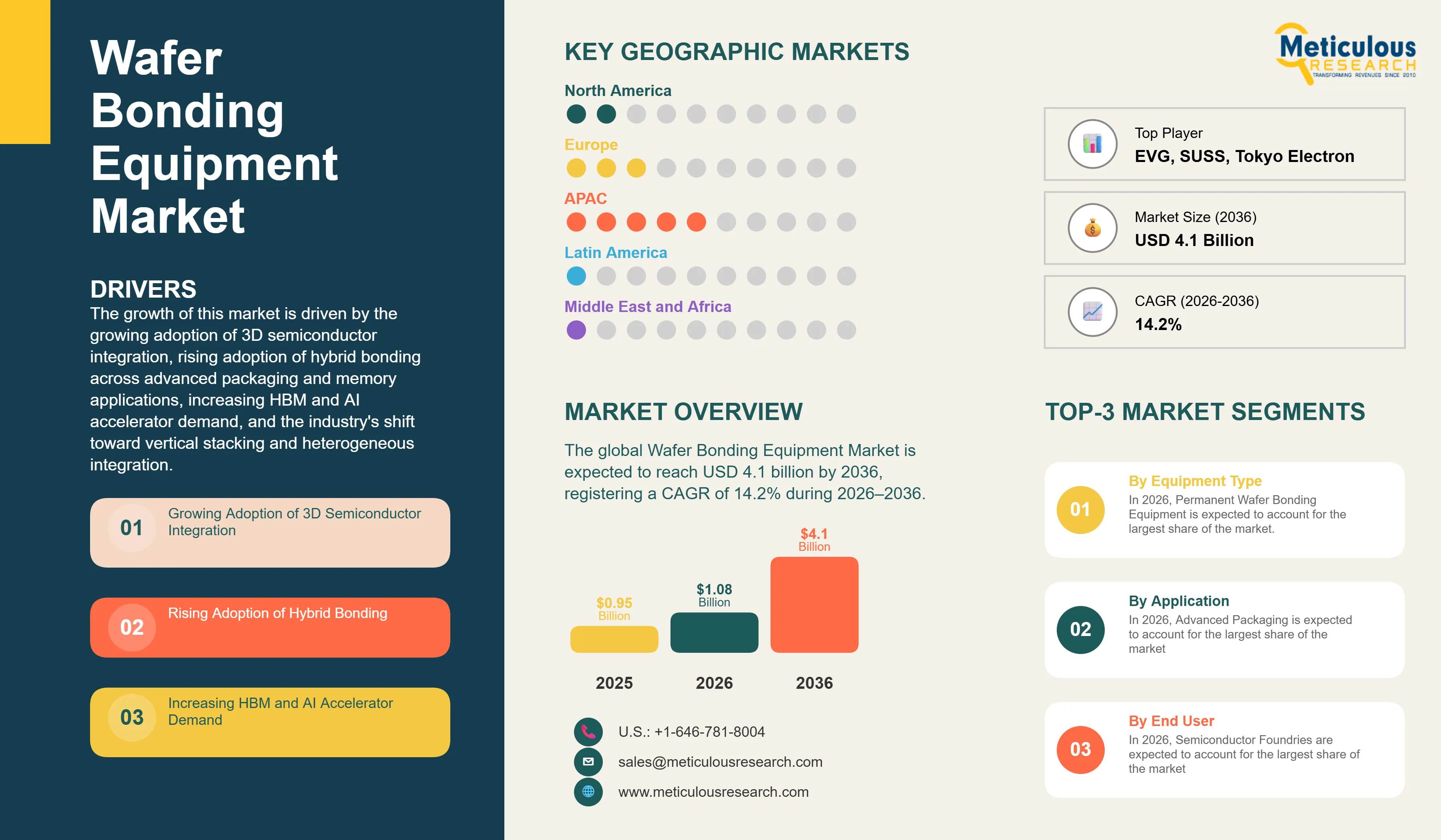
The global Wafer Bonding Equipment Market was valued at USD 0.95 billion in 2025 and is projected to reach USD 1.08 billion in 2026. The market is expected to reach USD 4.1 billion by 2036, registering a CAGR of 14.2% during the forecast period (2026-2036).
- Published
- Aug 2026
- Pages
- 289
- Format
- PDF + Excel
- Report ID
- MR-2137
- Base year
- 2025
- 2025 · BASELINE
- $950.0M
- 2036
- $4.10B
- CAGR 2026–2036
- 14.2%
2025 baseline · 2026–2036 forecast at 14.2% CAGR · hover a bar for the value
Key highlights
The global Wafer Bonding Equipment Market is projected to reach USD 4.1 billion by 2036, driven by growing adoption of 3D semiconductor integration and rising adoption of hybrid bonding across advanced packaging and memory applications.
Asia-Pacific is expected to account for the largest market share in 2026, while North America is projected to register the fastest growth during the forecast period.
By equipment type, Permanent Wafer Bonding Equipment is expected to account for the largest market share, whereas Hybrid Bonding Equipment is projected to witness the fastest growth through 2036.
By bonding technology, Direct/Fusion Bonding is expected to dominate the market, while Hybrid Bonding is projected to register the highest CAGR during the forecast period.
TSMC's SoIC hybrid bonding roadmap is advancing from a 6 micrometer pitch today toward 4.5 micrometers by 2029, illustrating the pace of equipment refresh being driven by continuous pitch scaling independent of underlying wafer volume growth.
Hybrid bonding adoption in HBM devices is expected to become near-universal by 2029 as HBM4 and HBM5 generations scale, creating significant long-term equipment demand tied to AI accelerator and high-performance computing growth.
Report summary
| Particulars | Details |
|---|---|
| Forecast Period | 2026-2036 |
| Base Year | 2025 |
| Estimated Year | 2026 |
| CAGR (Value) | 14.2% |
| Format | PDF, Excel & Cloud Portal · 289 pages |
| Market Size (Value) in 2026 | USD 1.08 Billion |
| Market Size (Value) in 2036 | USD 4.1 Billion |
| Segments Covered | By Equipment Type: Permanent Wafer Bonding Equipment (Direct/Fusion, Hybrid, Anodic, Eutectic, Adhesive, Thermocompression, Glass Frit), Temporary Wafer Bonding Equipment, Wafer Alignment & Positioning Equipment, Surface Preparation & Activation Equipment, Bond Annealing Equipment, Bond Inspection & Metrology Equipment, Wafer Bonding Automation & Material Handling Systems. · By Bonding Technology: Direct/Fusion Bonding, Hybrid Bonding, Anodic Bonding, Eutectic Bonding, Adhesive Bonding, Thermocompression Bonding, Glass Frit Bonding, Temporary Bonding & Debonding. · By Wafer Size: ≤150 mm, 200 mm, 300 mm, >300 mm. · By Substrate Material: Silicon, Silicon Carbide, Gallium Nitride, Gallium Arsenide, Glass, Sapphire, Other Substrate Materials. · By Application: 3D Semiconductor Integration, Advanced Packaging, MEMS & Sensors, Image Sensors, Power & Compound Semiconductors, Photonics & Optoelectronics. · By End User: Semiconductor Foundries, Integrated Device Manufacturers (IDMs), Memory Manufacturers, OSAT Providers, MEMS & Sensor Manufacturers, Compound Semiconductor Manufacturers, Research & Development Institutions. |
Report overview
Segments covered: equipment type, bonding technology, wafer size, substrate material, application, end user.
The Wafer Bonding Equipment Market comprises the systems used to prepare, align, bond, anneal, and inspect semiconductor wafers as part of 3D integration, advanced packaging, and MEMS and sensor manufacturing processes. Equipment spans permanent bonding systems for direct/fusion, hybrid, anodic, eutectic, adhesive, thermocompression, and glass frit bonding, as well as temporary bonding and debonding systems, wafer alignment and positioning tools, surface activation and cleaning systems, bond annealing equipment, and bond inspection and metrology systems used by semiconductor foundries, IDMs, OSAT providers, and MEMS and sensor manufacturers.
Demand is being reshaped by the semiconductor industry's shift from planar scaling toward vertical stacking, as chipmakers increasingly rely on wafer bonding to achieve heterogeneous integration and overcome the physical limits of traditional transistor scaling. SEMI reports that sub-10-micrometer-pitch die-to-wafer hybrid bonding is already in production for 3D integrated circuits, while the industry is actively developing hybrid bonding for high-bandwidth memory (HBM). SEMI's 2026 equipment outlook further projects global assembly and packaging equipment sales to increase 9.6% to US$6.7 billion in 2026, following 20.8% growth in 2025, driven by increasing device complexity and adoption of advanced and heterogeneous packaging for AI and HBM applications. These developments are directly expanding demand for high-precision wafer and die bonding, alignment, surface preparation, inspection, and metrology equipment.
The transition toward advanced memory is particularly important for wafer bonding equipment demand. SEMI projects worldwide 300mm memory fab equipment investment to reach US$52 billion in 2026, representing a 29% increase from 2025, while global 300mm memory capacity is expected to reach approximately 4.1 million wafers per month in 2026. Industry technology roadmaps show hybrid bonding moving toward increasingly fine pitches, with SEMI's 2025 hybrid-bonding roadmap identifying approximately 2 µm-to-sub-1 µm pitch targets for several future memory and logic applications. This increasing requirement for finer bonding pitches and tighter alignment tolerances is expected to drive equipment upgrades across wafer bonding, plasma activation, CMP, cleaning, overlay metrology, and inspection.
Leading foundries are also advancing hybrid-bonding technology for 3D logic integration. TSMC's SoIC platform and other advanced 3D integration technologies are increasing requirements for extremely precise wafer alignment, surface preparation, bonding, and inspection. As AI accelerators increasingly integrate logic and HBM through advanced packaging, the combination of rapidly expanding memory investment and increasingly fine-pitch bonding requirements is creating a structural equipment opportunity beyond conventional wafer-volume growth.
Report infographic
Market dynamics
8 factors across 4 forcesGrowing Adoption of 3D Semiconductor Integration
The semiconductor industry's shift from two-dimensional scaling toward three-dimensional stacking of memory, logic, and image sensor dies is a primary driver of demand for wafer bonding equipment. 3D integration enables higher transistor density and improved performance within a smaller footprint, and leading manufacturers including TSMC, Intel, and Samsung continue to expand proprietary hybrid bonding platforms such as SoIC and Foveros Direct to support this transition.
Rising Adoption of Hybrid Bonding
Hybrid bonding is rapidly displacing conventional micro-bump interconnects across image sensors, HBM, and advanced logic applications due to its ability to achieve finer pitch, lower thermal resistance, and reduced stack height. Image sensor applications are approaching near-total hybrid bonding penetration, and hybrid bonding is projected to be used in nearly all HBM devices by 2029, driving sustained demand for precision bonding, alignment, and inspection equipment across the industry.
Table of contents
14 chapters · 236 sections · 289 pages · click to expandSegmental analysis
| Segment | Largest share (2026) | Fastest growth (2026–2036) |
|---|---|---|
| By Equipment Type | Permanent Wafer Bonding Equipment | Hybrid Bonding Equipment |
| By Bonding Technology | Direct/Fusion Bonding | Hybrid Bonding |
| By Wafer Size | 300 mm | >300 mm |
| By Application | Advanced Packaging | 3D Semiconductor Integration |
| By End User | Semiconductor Foundries | Memory Manufacturers |
By Equipment Type
- Permanent Wafer Bonding Equipment is expected to account for the largest market share, reflecting its broad use across direct/fusion, hybrid, anodic, eutectic, and thermocompression bonding processes for advanced packaging and MEMS applications.
- However, Hybrid Bonding Equipment is projected to register the fastest growth during the forecast period, driven by its rapid expansion from image sensors into HBM and advanced logic manufacturing.
By Bonding Technology
- Direct/Fusion Bonding is expected to account for the largest market share, supported by its established, high-volume use across silicon-on-insulator, MEMS, and image sensor manufacturing.
- However, Hybrid Bonding is projected to register the highest CAGR during the forecast period, driven by accelerating adoption across HBM, 3D NAND, and advanced logic applications.
By Wafer Size
- The 300 mm segment is expected to account for the largest market share, reflecting its status as the dominant wafer size across leading-edge logic and memory fabs.
- However, the >300 mm segment is projected to register the highest CAGR during the forecast period, as equipment developers begin preparing for next-generation larger-format wafer processing to improve manufacturing economics.
By Application
- Advanced Packaging is expected to account for the largest market share, driven by rising wafer-to-wafer and die-to-wafer bonding demand for chiplet integration and heterogeneous integration architectures.
- However, 3D Semiconductor Integration is projected to register the highest CAGR during the forecast period, supported by accelerating hybrid bonding adoption across 3D memory and 3D logic applications tied to AI accelerator demand.
By End User
- Semiconductor Foundries are expected to account for the largest market share, led by leading-edge players expanding advanced packaging and hybrid bonding capacity to serve AI accelerator customers.
- However, Memory Manufacturers are projected to register the highest CAGR during the forecast period, as HBM producers scale hybrid bonding adoption across successive HBM4 and HBM5 generations.
Geographic analysis
Asia-Pacific
Largest shareIn 2026, Asia-Pacific is expected to account for the largest share of the global Wafer Bonding Equipment Market, supported by the region's concentration of leading foundries, memory manufacturers, and OSAT providers across Taiwan, South Korea, Japan, and China. According to SEMI, Asia-Pacific accounts for the overwhelming majority of global semiconductor manufacturing capacity, while Taiwan, South Korea, China, and Japan remain key centers for advanced logic, HBM, and advanced packaging production. SEMI projects global 300mm memory fab equipment investment to reach approximately US$52 billion in 2026, up 29% year over year, driven largely by AI-related demand for HBM and advanced memory. TSMC's advanced packaging operations in Taiwan and major HBM producers across South Korea and Japan are therefore supporting strong demand for wafer bonding, hybrid bonding, alignment, and inspection equipment. I would avoid saying these countries “account for the majority of global hybrid bonding capacity” unless you have a source specifically measuring hybrid-bonding capacity.
North America
Fastest growthHowever, North America is projected to register the highest CAGR during the forecast period, driven by expanding domestic advanced packaging investment in the United States, supported by CHIPS Act-related incentives, as well as growing demand for AI accelerator and high-performance computing chips that rely increasingly on advanced packaging and HBM integration. In January 2025, the U.S. Department of Commerce announced approximately US$1.4 billion in CHIPS National Advanced Packaging Manufacturing Program (NAPMP) awards to strengthen domestic advanced packaging capabilities, including investments in packaging R&D, substrates, and manufacturing infrastructure. TSMC is also investing more than US$100 billion to expand its U.S. semiconductor manufacturing ecosystem, including three additional fabs, two advanced packaging facilities, and an R&D center in Arizona. These investments are expected to accelerate domestic adoption of high-precision wafer bonding, hybrid bonding, die-to-wafer bonding, surface activation, and bond inspection technologies.
Competitive landscape
The global Wafer Bonding Equipment Market is moderately consolidated, with competition among established semiconductor equipment manufacturers and specialized wafer bonding technology providers. Companies compete primarily on bond pitch precision, alignment accuracy, throughput, and the ability to support the transition from micro-bump to hybrid bonding interconnects for advanced packaging customers.
Leading market participants are investing in finer-pitch hybrid bonding platforms, improved surface activation and inspection capabilities, and expanded production capacity to meet growing demand from HBM and advanced logic manufacturers. Strategic partnerships with leading foundries and memory manufacturers, along with continued R&D investment in sub-5 micrometer pitch bonding technology, remain key strategies adopted by major vendors.
The report provides a comprehensive competitive assessment of the leading companies operating in the global Wafer Bonding Equipment Market. The key players profiled in the report include EV Group (EVG), SUSS MicroTec SE, Tokyo Electron Limited, Applied Materials, Inc., Besi Netherlands B.V., ASMPT Limited, KLA Corporation, Ayumi Industry Co., Ltd., Mitsubishi Heavy Industries, Ltd., Panasonic Industry Co., Ltd., Hanmi Semiconductor Co., Ltd., SET Corporation, AML Automation, SMEE, and NIL Technology ApS.
- EV Group (EVG)
- SUSS MicroTec SE
- Tokyo Electron Limited
- Applied Materials, Inc.
- Besi Netherlands B.V.
- ASMPT Limited
- KLA Corporation
- Ayumi Industry Co., Ltd.
- Mitsubishi Heavy Industries, Ltd.
- Panasonic Industry Co., Ltd.
- Hanmi Semiconductor Co., Ltd.
- SET Corporation
- AML Automation
- SMEE
- NIL Technology ApS
Frequently asked questions
The global Wafer Bonding Equipment Market is estimated at USD 1.08 billion in 2026.
Cite this report
Meticulous Research. (2026). Wafer Bonding Equipment Market - Global Opportunity Analysis and Industry Forecast to 2036 (Report No. MR-2137). Meticulous Market Research Pvt. Ltd. https://www.meticulousresearch.com/product/wafer-bonding-equipment-market-6820