Chiplet Assembly Equipment Market
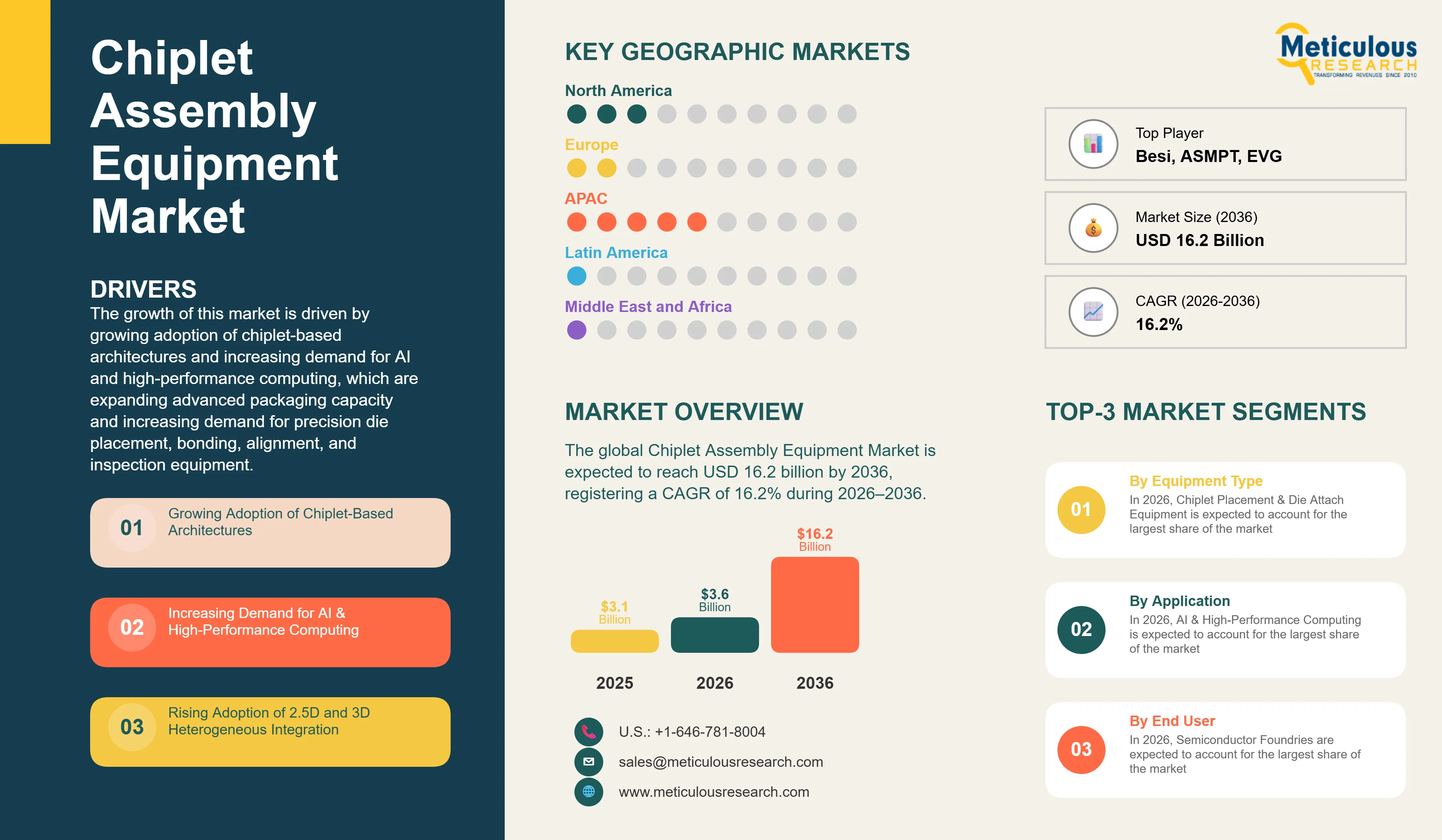
The global Chiplet Assembly Equipment Market was valued at USD 3.1 billion in 2025 and is projected to reach USD 3.6 billion in 2026. The market is expected to reach USD 16.2 billion by 2036, registering a CAGR of 16.2% during the forecast period (2026-2036).
- Published
- Aug 2026
- Pages
- 310
- Format
- PDF + Excel
- Report ID
- MR-2136
- Base year
- 2025
- 2025 · BASELINE
- $3.10B
- 2036
- $16.20B
- CAGR 2026–2036
- 16.2%
2025 baseline · 2026–2036 forecast at 16.2% CAGR · hover a bar for the value
Key highlights
The global Chiplet Assembly Equipment Market is projected to reach USD 16.2 billion by 2036, driven by growing adoption of chiplet-based architectures and increasing demand for AI and high-performance computing.
Asia-Pacific is expected to account for the largest market share in 2026, while North America is projected to register the fastest growth during the forecast period.
By equipment type, Chiplet Placement & Die Attach Equipment is expected to account for the largest market share, whereas Chiplet Bonding Equipment is projected to witness the fastest growth through 2036.
By assembly technology, 2.5D Assembly is expected to dominate the market, while Hybrid Bonding is projected to register the highest CAGR during the forecast period.
SEMI counted 750 assembly and test facilities worldwide in July 2025, an increase of 70 sites from its previous count, reflecting the rapid buildout of chiplet and advanced packaging assembly capacity that is directly expanding demand for precision assembly equipment.
TSMC's plan to expand CoWoS advanced packaging capacity toward 100, 000-120,000 wafers per month by 2026, alongside major capacity investments such as SK hynix's USD 3.87 billion advanced packaging facility in Indiana, is expected to create significant long-term equipment demand.
Report summary
| Particulars | Details |
|---|---|
| Forecast Period | 2026-2036 |
| Base Year | 2025 |
| Estimated Year | 2026 |
| CAGR (Value) | 16.2% |
| Format | PDF, Excel & Cloud Portal · 310 pages |
| Market Size (Value) in 2026 | USD 3.6 Billion |
| Market Size (Value) in 2036 | USD 16.2 Billion |
| Segments Covered | By Equipment Type: Chiplet Placement & Die Attach Equipment (High-Precision Die Bonders, Pick-and-Place Systems, Flip-Chip Bonders, Die-to-Wafer/Die-to-Die Placement Systems), Chiplet Bonding Equipment (Hybrid, Thermocompression, Direct, Solder-Based, Copper-to-Copper), Wafer-to-Wafer & Die-to-Wafer Bonding Equipment, Alignment & Positioning Equipment, Surface Preparation & Activation Equipment, Inspection & Metrology Equipment, Chiplet Handling & Automation Equipment, Process Control & Software. · By Assembly Technology: Die-to-Die, Die-to-Wafer, Wafer-to-Wafer, 2.5D, 3D, Hybrid Bonding, Thermocompression Bonding, Flip-Chip Assembly. By Placement Accuracy: >10 µm, 5-10 µm, 1-5 µm, 0.5-1 µm, <0.5 µm, Sub-100 nm Precision. · By Wafer Size: ≤150 mm, 200 mm, 300 mm, >300 mm. By Packaging Architecture: 2.5D Packaging (Silicon/Organic/Glass Interposer-Based), 3D Packaging (3D Logic Stacking, 3D Memory Stacking, Logic-on-Logic, Logic-on-Memory), Fan-Out Chiplet Packaging, Bridge-Based Chiplet Packaging, System-in-Package (SiP), Heterogeneous Integration. · By Application: AI & High-Performance Computing, High Bandwidth Memory, Advanced Logic, Networking & Data Center Semiconductors, Consumer & Mobile Electronics, Automotive Electronics. · By End User: Semiconductor Foundries, IDMs, Memory Manufacturers, OSAT Providers, Advanced Packaging Specialists, Semiconductor R&D Organizations. |
| Countries Covered | North America: U.S., Canada. · Europe: Germany, France, U.K., Netherlands, Belgium, Italy, Rest of Europe. · Asia-Pacific: Taiwan, China, South Korea, Japan, Singapore, India, Malaysia, Vietnam, Rest of Asia-Pacific. · Latin America: Brazil, Mexico, Argentina, Rest of Latin America. · Middle East & Africa: Israel, UAE, Saudi Arabia, South Africa, Rest of Middle East & Africa. |
| Key Companies | BE Semiconductor Industries N.V. (Besi), ASMPT Limited, EV Group (EVG), SUSS MicroTec SE, Applied Materials, Inc., Tokyo Electron Limited, Kulicke & Soffa Industries, Inc., Tokyo Seimitsu Co., Ltd., Disco Corporation, Onto Innovation Inc., KLA Corporation, SET Corporation, Hanmi Semiconductor Co., Ltd., and Shibaura Mechatronics Corporation. |
Report overview
Segments covered: equipment type, assembly technology, wafer size, application, end user, placement accuracy, packaging architecture.
The Chiplet Assembly Equipment Market comprises the systems used to place, align, bond, inspect, and handle chiplets as semiconductor manufacturers shift from monolithic system-on-chip designs toward modular architectures built from multiple interoperable dies within a single package. Equipment spans high-precision die bonders, pick-and-place systems, hybrid and thermocompression bonding equipment, wafer-to-wafer and die-to-wafer bonders, sub-micron alignment and positioning systems, surface preparation and activation equipment, and inspection and metrology systems used by semiconductor foundries, IDMs, and OSAT providers to assemble 2.5D and 3D chiplet-based packages.
Demand for chiplet assembly equipment is being driven by the rapid expansion of semiconductor assembly and test capacity worldwide. According to the latest SEMI and TechSearch International Worldwide Assembly & Test Facility Database released in July 2026, more than 820 semiconductor assembly and test facilities are now tracked globally, up from 750 facilities in the 2025 edition. The database also expands coverage of packaging technologies and end markets, reflecting continued investment in advanced packaging infrastructure. This expansion is being reinforced by strong AI-driven investment in advanced packaging: SEMI reported that global semiconductor equipment billings reached US$135.1 billion in 2025, up 15% year over year, while assembly and packaging equipment sales increased 21% as advanced packaging adoption expanded.
The buildout is particularly concentrated around AI accelerators and HBM. SEMI projects global 300mm memory equipment investment to reach approximately US$52 billion in 2026, a 29% increase from 2025, driven by AI-related demand for HBM and other advanced memory technologies. SK hynix is investing approximately US$3.87 billion in West Lafayette, Indiana, to establish an advanced packaging and R&D facility for next-generation HBM products, with the facility expected to create more than 1,000 jobs. These investments are increasing demand for precision die bonding, thermocompression and hybrid bonding, advanced alignment, inspection, and metrology equipment required for chiplet and HBM-based package assembly.
Report infographic
Market dynamics
8 factors across 4 forcesGrowing Adoption of Chiplet-Based Architectures
The semiconductor industry's shift from monolithic system-on-chip designs toward modular chiplet-based architectures is the primary driver of demand for chiplet assembly equipment. Chiplet designs allow manufacturers to combine dies fabricated at different process nodes within a single package, improving yield economics and enabling faster product development cycles, directly increasing the volume of precision die placement, bonding, and inspection steps required per package.
Increasing Demand for AI & High-Performance Computing
The rapid growth of AI accelerator, GPU, and high-performance computing chip production is driving substantial demand for chiplet assembly equipment. As leading foundries scale CoWoS and similar advanced packaging platforms toward 100,000-120,000 wafers per month by 2026 to meet AI accelerator demand, equipment providers are seeing sustained order growth for high-precision die bonders, hybrid bonding systems, and inspection equipment.
Table of contents
15 chapters · 269 sections · 310 pages · click to expandSegmental analysis
| Segment | Largest share (2026) | Fastest growth (2026–2036) |
|---|---|---|
| By Equipment Type | Chiplet Placement & Die Attach Equipment | Chiplet Bonding Equipment |
| By Assembly Technology | 2.5D Assembly | Hybrid Bonding |
| By Placement Accuracy | 1-5 µm | Sub-100 nm Precision |
| By Application | AI & High-Performance Computing | High Bandwidth Memory |
| By End User | Semiconductor Foundries | Memory Manufacturers |
By Equipment Type
- Chiplet Placement & Die Attach Equipment is expected to account for the largest market share, reflecting its foundational role across nearly all chiplet assembly workflows through high-precision die bonders and pick-and-place systems.
- However, Chiplet Bonding Equipment, particularly hybrid bonding systems, is projected to register the fastest growth during the forecast period, driven by accelerating hybrid bonding adoption for HBM and logic integration.
By Assembly Technology
- 2.5D Assembly is expected to account for the largest market share, supported by its widespread commercial use in AI accelerator and HBM packaging platforms such as CoWoS.
- However, Hybrid Bonding is projected to register the highest CAGR during the forecast period, driven by its expanding role in 3D logic and memory stacking applications.
By Placement Accuracy
- The 1-5 µm segment is expected to account for the largest market share, reflecting the accuracy level required by most current-generation flip-chip and 2.5D chiplet assembly processes.
- However, the Sub-100 nm Precision segment is projected to register the highest CAGR during the forecast period, driven by the increasing precision requirements of hybrid bonding for next-generation HBM and 3D logic stacking.
By Application
- AI & High-Performance Computing is expected to account for the largest market share, reflecting the outsized role AI accelerators, GPUs, and custom AI ASICs play in driving chiplet assembly equipment demand.
- However, High Bandwidth Memory is projected to register the highest CAGR during the forecast period, as HBM manufacturers scale stacking and HBM-to-logic integration through successive HBM4 and next-generation HBM designs.
By End User
- Semiconductor Foundries are expected to account for the largest market share, led by leading-edge players expanding chiplet assembly capacity to serve AI accelerator customers.
- However, Memory Manufacturers are projected to register the highest CAGR during the forecast period, as HBM producers invest heavily in dedicated assembly capacity such as SK hynix's Indiana facility.
Geographic analysis
Asia-Pacific
Largest shareIn 2026, Asia-Pacific is expected to account for the largest share of the global Chiplet Assembly Equipment Market, supported by the region's concentration of leading foundries, OSAT providers, and advanced memory manufacturers across Taiwan, South Korea, Japan, and China. According to SEMI's 2026 Worldwide Assembly & Test Facility Database, Asia-Pacific remains the dominant center of semiconductor backend manufacturing, with more than 820 assembly and test facilities tracked globally and major concentrations across Taiwan, China, South Korea, Japan, and Southeast Asia. SEMI also reports that 64 new semiconductor fabs are expected to become operational across Asia by 2029, demonstrating the region's continued expansion of semiconductor manufacturing infrastructure. Amkor's US$1.6 billion Vietnam campus, which includes advanced system-in-package and memory production capabilities, further strengthens Southeast Asia's role in advanced packaging.
North America
Fastest growthHowever, North America is projected to register the highest CAGR during the forecast period, driven by substantial domestic investment in advanced semiconductor packaging and chiplet technologies. In January 2025, the U.S. Department of Commerce finalized US$1.4 billion in CHIPS National Advanced Packaging Manufacturing Program (NAPMP) awards, including US$1.1 billion for the National Advanced Packaging Manufacturing Program facility in Arizona and US$300 million for advanced substrate and materials projects. TSMC is also investing more than US$100 billion in expanding its U.S. semiconductor manufacturing ecosystem, including three additional fabs, two advanced packaging facilities, and an R&D center in Arizona. Furthermore, in July 2026, Amkor and NVIDIA announced a US$1.5 billion multi-year advanced packaging and development agreement to expand Amkor's U.S. advanced packaging capacity for next-generation AI and accelerated-computing platforms. These investments are expected to accelerate demand for precision die bonders, hybrid and thermocompression bonding equipment, advanced alignment systems, inspection and metrology equipment, and other chiplet assembly technologies across North America.
Competitive landscape
The global Chiplet Assembly Equipment Market is moderately consolidated, with competition among established semiconductor assembly equipment manufacturers and specialized bonding and inspection technology providers. Companies compete primarily on placement accuracy, bonding pitch precision, throughput, and the ability to support multiple chiplet assembly technologies within a single production line.
Leading market participants are investing in higher-precision die bonders, expanded hybrid bonding capacity, and advanced inspection and metrology systems to meet growing demand from AI accelerator and HBM manufacturers. Strategic partnerships with leading foundries and memory manufacturers, along with continued R&D investment in sub-micron and sub-100-nanometer placement technology, remain key strategies adopted by major vendors.
The report provides a comprehensive competitive assessment of the leading companies operating in the global Chiplet Assembly Equipment Market. The key players profiled in the report include BE Semiconductor Industries N.V. (Besi), ASMPT Limited, EV Group (EVG), SUSS MicroTec SE, Applied Materials, Inc., Tokyo Electron Limited, Kulicke & Soffa Industries, Inc., Tokyo Seimitsu Co., Ltd., Disco Corporation, Onto Innovation Inc., KLA Corporation, SET Corporation, Hanmi Semiconductor Co., Ltd., and Shibaura Mechatronics Corporation.
- BE Semiconductor Industries N.V. · Besi
- ASMPT Limited
- EV Group (EVG)
- SUSS MicroTec SE
- Applied Materials, Inc.
- Tokyo Electron Limited
- Kulicke & Soffa Industries, Inc.
- Tokyo Seimitsu Co., Ltd.
- Disco Corporation
- Onto Innovation Inc.
- KLA Corporation
- SET Corporation
- Hanmi Semiconductor Co., Ltd.
- Shibaura Mechatronics Corporation
Frequently asked questions
The global Chiplet Assembly Equipment Market is estimated at USD 3.6 billion in 2026.
Cite this report
Meticulous Research. (2026). Chiplet Assembly Equipment Market Global Opportunity Analysis and Industry Forecast to 2036 (Report No. MR-2136). Meticulous Market Research Pvt. Ltd. https://www.meticulousresearch.com/product/chiplet-assembly-equipment-market-6819