Resources
About Us
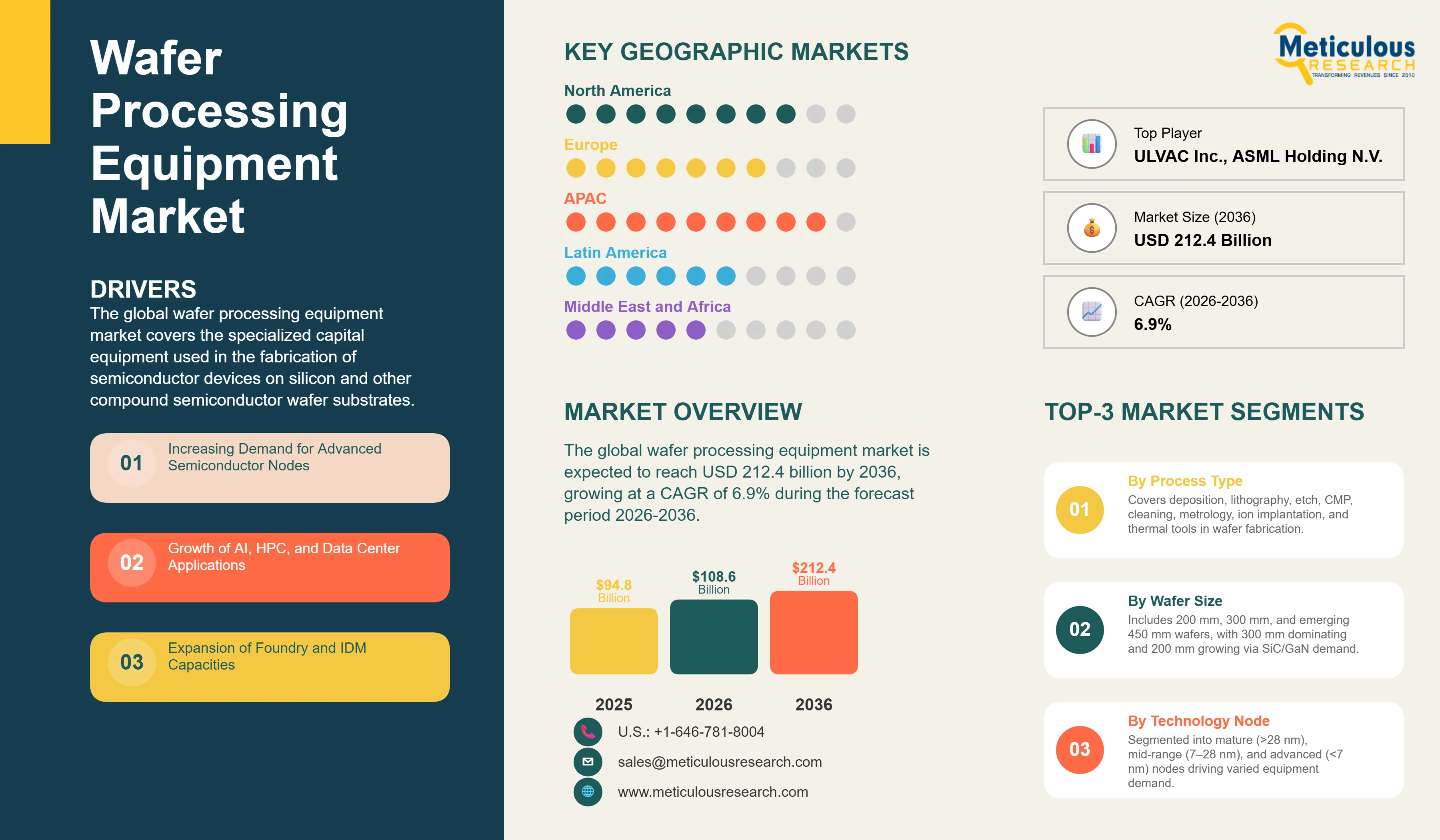
The global wafer processing equipment market was valued at USD 94.8 billion in 2025. This market is expected to reach USD 212.4 billion by 2036 from an estimated USD 108.6 billion in 2026, growing at a CAGR of 6.9% during the forecast period 2026-2036.
 Click here to: Get Free Sample Pages of this Report
The global wafer processing equipment market covers the specialized capital equipment used in the fabrication of semiconductor devices on silicon, silicon carbide, gallium nitride, and other compound semiconductor wafer substrates. This encompasses the full range of front-end-of-line process equipment including deposition systems for chemical vapor deposition, physical vapor deposition, and atomic layer deposition, photolithography systems spanning deep ultraviolet and extreme ultraviolet exposure platforms, dry and wet etching equipment, chemical mechanical planarization systems, wafer cleaning tools, inspection and metrology platforms, ion implantation systems, and thermal processing equipment that collectively perform the hundreds to thousands of process steps required to fabricate advanced logic, memory, power, and analog semiconductor devices.
The growth of the global wafer processing equipment market is primarily driven by the semiconductor industry's continued advancement along the technology node roadmap toward 3 nm, 2 nm, and sub-2 nm logic nodes that require progressively more sophisticated and higher-capital-intensity process equipment per wafer layer, and the unprecedented global wave of fab investment programs being funded through the U.S. CHIPS and Science Act, the EU Chips Act, and national semiconductor manufacturing investment initiatives in Japan, South Korea, India, and Taiwan that are creating the largest sustained increase in semiconductor manufacturing capacity investment in the industry's history. The AI-driven surge in advanced logic chip demand for training accelerators and inference processors at TSMC, Samsung Foundry, and Intel Foundry is generating the strongest advanced node capacity expansion cycle in recent memory, with each new leading-edge logic fab representing USD 15 to 25 billion of process equipment procurement.
Two significant opportunities are shaping the market's long-term trajectory. The rapid growth of compound semiconductor manufacturing, particularly silicon carbide for EV power electronics and gallium nitride for RF and power conversion applications, represents a fast-growing and high-value adjacent market for wafer processing equipment that is expanding the addressable market beyond traditional silicon device manufacturing and requiring specialized equipment adaptations for the different substrate properties, process temperatures, and chemistry requirements of SiC and GaN fabrication. The continuing advancement toward and beyond the 2 nm technology node, requiring the adoption of High-NA EUV lithography and increasingly complex multi-patterning and gate-all-around transistor process sequences, is driving equipment replacement cycles and new equipment procurement at leading-edge fabs at the highest per-wafer-layer equipment cost intensity in semiconductor manufacturing history.
|
Parameters |
Details |
|
Market Size by 2036 |
USD 212.4 Billion |
|
Market Size in 2026 |
USD 108.6 Billion |
|
Market Size in 2025 |
USD 94.8 Billion |
|
Revenue Growth Rate (2026-2036) |
CAGR of 6.9% |
|
Dominating Process Type |
Deposition Equipment |
|
Fastest Growing Process Type |
Lithography Equipment (EUV) |
|
Dominating Wafer Size |
300 mm |
|
Fastest Growing Wafer Size |
200 mm (SiC/GaN applications) |
|
Dominating Technology Node |
Mature Nodes (>28 nm) |
|
Fastest Growing Technology Node |
Advanced Nodes (<7 nm) |
|
Dominating Material Type |
Silicon (Si) |
|
Fastest Growing Material Type |
Silicon Carbide (SiC) |
|
Dominating Application |
Logic Devices |
|
Fastest Growing Application |
Power Devices |
|
Dominating End User |
Foundries |
|
Fastest Growing End User |
IDMs |
|
Dominating Geography |
Asia-Pacific |
|
Fastest Growing Geography |
North America |
|
Base Year |
2025 |
|
Forecast Period |
2026 to 2036 |
Ramp of EUV and High-NA EUV Lithography Driving Premium Equipment Demand
The progressive transition of advanced logic manufacturing from DUV multi-patterning to EUV single-exposure lithography at the 5 nm node and below, and the commercial introduction of High-NA EUV systems for sub-2 nm node production, represents the most commercially significant equipment investment trend in the semiconductor industry. ASML's EUV scanner is the highest-value single piece of capital equipment in any manufacturing industry, with Low-NA EUV systems priced at approximately USD 150 to 200 million per unit and High-NA EUV EXE:5000 systems exceeding USD 350 million per unit, and the accelerating deployment of EUV across TSMC, Samsung Foundry, and Intel Foundry's advanced node capacity programs is generating extraordinary revenue growth for ASML. The adoption of High-NA EUV, with its 0.55 numerical aperture enabling the resolution required for patterns below 8 nanometers at single exposure, is creating demand for the entirely new photoresist, underlayer, and ancillary chemistry platforms required for High-NA compatibility.
The EUV ramp is creating cascading demand across the wafer processing equipment ecosystem beyond lithography itself. EUV-exposed resist patterns require different etch process conditions than DUV patterns, driving etch equipment upgrades at leading-edge fabs. The thinner resist films compatible with High-NA EUV require more selective and more controlled etch processes, driving ALD-based conformal deposition and atomic layer etch equipment adoption. The increasing layer count of leading-edge logic devices and the complexity of gate-all-around nanosheet transistor process flows are driving growth in ALD, CVD, and selective etch equipment procurement that benefits Applied Materials, Lam Research, and Tokyo Electron across their respective process equipment portfolios.
Compound Semiconductor Equipment Growth Driven by SiC and GaN
The rapid commercial expansion of silicon carbide power device manufacturing for electric vehicle inverters, industrial power conversion, and EV charging infrastructure is creating a significant and fast-growing new market segment for wafer processing equipment adapted or purpose-designed for SiC substrate fabrication. SiC wafer processing differs substantially from silicon processing in requiring higher oxidation and deposition temperatures, specialized ion implantation conditions for dopant activation in the wide-bandgap SiC lattice, different etching chemistry and plasma conditions for SiC etching, and high-temperature post-implant annealing at temperatures exceeding 1,600 degrees Celsius that require specialized thermal processing equipment not used in silicon fabs. The rapid scaling of SiC device manufacturers including Wolfspeed, ON Semiconductor, STMicroelectronics, Infineon, and ROHM from 150 mm to 200 mm wafer processing is driving substantial equipment procurement at each facility upgrade and new capacity addition.
Applied Materials has developed a suite of SiC-specific process equipment including SiC epitaxial deposition systems, SiC ion implantation tools, and SiC-optimized CMP and cleaning equipment that are qualified and deployed at major SiC device manufacturers globally. Lam Research's SiC-compatible plasma etch and deposition platforms and Tokyo Electron's SiC thermal processing equipment are similarly positioned to capture the growing SiC equipment market. The transition of GaN-on-silicon and GaN-on-SiC RF and power device manufacturing from R&D to high-volume production is creating parallel equipment demand growth for GaN-compatible deposition, etch, and inspection platforms that represents an important long-term equipment market expansion opportunity.
Geographic Diversification of Semiconductor Manufacturing Driving Equipment Demand
The structural shift in semiconductor manufacturing geography driven by the U.S. CHIPS Act, EU Chips Act, and national manufacturing incentive programs is creating a once-in-a-generation wave of new fab construction across geographies that have historically had limited semiconductor manufacturing capacity, generating unprecedented equipment procurement demand from new facility ramps that extend well beyond the traditional Asia-Pacific equipment demand concentration. TSMC's Arizona fab complex, Samsung's Texas facilities, Intel's Ohio and Arizona fabs, Micron's U.S. expansion, GlobalFoundries' U.S. programs, and TSMC's Dresden JV with Bosch, Infineon, and NXP collectively represent hundreds of billions of dollars in new fab investment requiring equipment procurement programs that are sustaining and growing equipment manufacturer revenue through periods when cyclical demand softness at established Asian fabs would otherwise compress total market volumes.
The geographic diversification trend is also creating new equipment installation and service market opportunities as equipment manufacturers establish local applications engineering, service, and spare parts logistics infrastructure to support fab ramps in new locations. Applied Materials, Lam Research, Tokyo Electron, and KLA Corporation are all expanding their North American and European service and applications organizations to support the new fab customer base, representing investments in market presence that will sustain long-term revenue from the installed base of equipment at new fab locations through their multi-decade operational lifetimes.
Increasing Demand for Advanced Semiconductor Nodes
The primary driver of the global wafer processing equipment market is the semiconductor industry's sustained advancement toward sub-3 nm and sub-2 nm logic technology nodes that require progressively more capable, more numerous, and higher-cost process equipment per manufactured chip. Each successive technology node generation increases the number of mask layers required per chip, adding multiple deposition, lithography, etch, and CMP process steps to the manufacturing sequence and expanding the equipment capital investment required per wafer fab proportionally. The transition to gate-all-around nanosheet transistor architectures at the 2 nm node and below involves entirely new epitaxial deposition, selective etch, and thermal processing sequences that require equipment configurations and capabilities not needed for FinFET devices, creating mandatory equipment upgrade and replacement cycles at leading-edge fabs that directly drive equipment procurement demand. The AI chip demand driven by foundation model training and inference infrastructure buildout at hyperscale data centers is generating unprecedented demand for advanced logic chips from TSMC, Samsung Foundry, and Intel Foundry that is sustaining leading-edge fab utilization and capital investment at historically high levels through the forecast period.
Expansion of Foundry and IDM Capacities
The global expansion of both pure-play foundry capacity and integrated device manufacturer production programs represents a sustained structural demand driver for wafer processing equipment that is operating independently of the cyclical demand fluctuations that have historically dominated semiconductor equipment market dynamics. TSMC's announced capital expenditure of approximately USD 32 to 38 billion annually through the mid-2020s, dedicated primarily to equipment procurement for advancing and expanding its leading-edge and mature node manufacturing capacity, represents the single largest annual equipment procurement program globally and sets a sustained demand floor for the equipment suppliers serving TSMC's technology transitions. Samsung Semiconductor's parallel capacity investment program, Intel's IDM 2.0 strategy investing heavily in its foundry capabilities across U.S. and European facilities, and the GlobalFoundries, UMC, and SMIC capacity expansion programs collectively create a multi-supplier equipment procurement market of extraordinary scale and geographic diversity that sustains the wafer processing equipment market at elevated investment levels throughout economic cycles.
Growth in Compound Semiconductors (SiC, GaN)
The commercial expansion of silicon carbide and gallium nitride semiconductor manufacturing for EV power electronics, EV charging infrastructure, industrial power conversion, and 5G RF applications represents a large and rapidly growing adjacent market opportunity for wafer processing equipment manufacturers whose silicon-optimized equipment portfolios require SiC and GaN-specific product development to address the unique substrate and process chemistry requirements of compound semiconductor fabrication. The global SiC power device market is growing at over 30% annually driven by the EV industry's adoption of SiC MOSFETs in inverters, on-board chargers, and DC-DC converters for their efficiency advantages over silicon IGBTs, and the resulting SiC device manufacturing capacity expansion programs at Wolfspeed, ON Semiconductor, STMicroelectronics, and Infineon are generating very large SiC-specific equipment procurement programs. Equipment companies including Applied Materials, Lam Research, and Veeco that have developed SiC-qualified process equipment are capturing premium-valued procurement from SiC manufacturers who require equipment with demonstrated SiC process compatibility and performance specifications that general-purpose silicon equipment cannot consistently achieve.
Increasing Investment in Regional Semiconductor Manufacturing
The global strategic investment in regional semiconductor manufacturing capacity outside the traditional Taiwan-Korea-Japan concentration in Asia-Pacific represents a multi-decade structural demand expansion for wafer processing equipment that will sustain above-trend equipment market growth through the 2026 to 2036 forecast period and well beyond. The CHIPS and Science Act's USD 52 billion in manufacturing incentives is enabling fab construction programs by TSMC, Samsung, Intel, Micron, GlobalFoundries, and multiple smaller specialized manufacturers that would not have been economically viable without public subsidy, translating policy intent into concrete equipment procurement programs. The EU Chips Act's EUR 43 billion investment mobilization is enabling the TSMC Dresden JV, Intel Magdeburg, and multiple European IDM capacity expansions that are establishing new semiconductor manufacturing clusters in Germany, Ireland, the Netherlands, and Poland that will require sustained equipment support across their operational lifetimes. Japan's RAPIDUS national semiconductor program, targeting sub-2 nm logic manufacturing at Chitose in partnership with IBM, represents an important additional new fab construction program generating leading-edge equipment procurement demand.
By Process Type: In 2026, Deposition Equipment to Dominate
Based on process type, the global wafer processing equipment market is segmented into deposition equipment, lithography equipment, etching equipment, CMP equipment, wafer cleaning equipment, inspection and metrology equipment, ion implantation equipment, thermal processing equipment, and other processing equipment. In 2026, the deposition equipment segment is expected to account for the largest share of the global wafer processing equipment market. The large share of this segment is attributed to deposition processes encompassing CVD, PVD, and ALD collectively representing the most equipment-intensive and highest capital expenditure category within the wafer fabrication process flow, with multiple deposition steps required at each device layer for gate dielectric, metal contact, barrier, interconnect, and hardmask film deposition applications across hundreds of process layers in leading-edge logic chips. Applied Materials is the global leader in deposition equipment, with its Centura and Endura platforms dominating CVD, PVD, and ALD tool procurement across leading foundries and IDMs.
However, the lithography equipment segment is poised to register the highest CAGR during the forecast period. The high growth of this segment is attributed to the accelerating EUV scanner installation rates at TSMC, Samsung Foundry, and Intel Foundry for advanced node capacity expansion, the introduction of High-NA EUV EXE:5000 systems at Intel's Intel 18A and future nodes at very high per-unit prices exceeding USD 350 million, and the continuous increase in EUV scanner count per wafer fab as EUV layer count per chip grows at each successive advanced technology node.
By Wafer Size: In 2026, 300 mm to Hold the Largest Share
Based on wafer size, the global wafer processing equipment market is segmented into 200 mm, 300 mm, and 450 mm (emerging). In 2026, the 300 mm segment is expected to account for the largest share of the global wafer processing equipment market. The dominance of 300 mm reflects the industry-standard wafer size for all leading-edge and advanced logic and memory semiconductor manufacturing, with TSMC, Samsung, SK Hynix, Micron, Intel, and all major high-volume semiconductor manufacturers operating 300 mm fabs that consume the large majority of global semiconductor equipment procurement. The superior economics of 300 mm manufacturing relative to 200 mm for high-volume silicon device production, driven by the larger die count per wafer and the automation advantages of 300 mm AMHS-equipped facilities, ensure 300 mm's continued dominance as the production wafer size for the foreseeable forecast horizon.
However, the 200 mm segment is projected to register significant growth during the forecast period. This growth is driven by the expansion of SiC and GaN compound semiconductor manufacturing, which is currently conducted primarily on 150 mm and 200 mm substrates due to the limited availability and high cost of larger-diameter SiC wafers, the sustained high demand for mature-node silicon devices fabricated at 200 mm fabs for automotive, industrial, and IoT applications, and the significant new 200 mm fab investment programs being driven by mature-node supply shortages experienced during the 2021 to 2023 semiconductor supply crisis.
By Technology Node: In 2026, Mature Nodes to Hold the Largest Share
Based on technology node, the global wafer processing equipment market is segmented into advanced nodes (below 7 nm), mid-range nodes (7 to 28 nm), and mature nodes (above 28 nm). In 2026, the mature nodes segment is expected to account for the largest share of the global wafer processing equipment market. The dominance of mature nodes reflects the very large global installed base of semiconductor manufacturing capacity at 28 nm and above serving the automotive, industrial, IoT, consumer electronics, and analog and mixed-signal device markets that represent the majority of global semiconductor unit production volume. The large number of mature-node fabs globally, including those operated by TSMC, GlobalFoundries, UMC, SMIC, and numerous IDMs and specialty manufacturers, collectively generates the highest aggregate equipment maintenance, upgrade, and replacement procurement volumes even though individual transaction values are lower than advanced node equipment.
However, the advanced nodes segment is projected to register the highest CAGR during the forecast period. This growth is driven by the very high per-layer and per-wafer equipment capital intensity of sub-7 nm manufacturing, the progressive ramp of multiple new leading-edge logic fabs at TSMC, Samsung, and Intel across the forecast period, and the growing layer count per chip at each successive advanced node that expands equipment requirements per wafer fab even at constant wafer volume.
By Material Type: In 2026, Silicon to Hold the Largest Share
Based on material type, the global wafer processing equipment market is segmented into silicon, silicon carbide, gallium nitride, and other compound semiconductors. In 2026, the silicon segment is expected to account for the largest share of the global wafer processing equipment market. Silicon's overwhelming dominance reflects its position as the substrate material for the vast majority of global semiconductor production, encompassing all leading-edge logic and memory devices, the majority of analog and power semiconductor production, and nearly all foundry services. The decades-long optimization of silicon wafer processing equipment and process chemistry, the availability of 300 mm silicon substrates at low cost, and silicon's excellent thermal and electrical properties for most semiconductor device categories ensure its continued dominance through the forecast period.
However, the silicon carbide segment is projected to register the highest CAGR during the forecast period. This growth is driven by the explosive commercial expansion of SiC power device manufacturing for EV inverters and chargers, the planned transition of major SiC manufacturers from 150 mm to 200 mm wafer processing at multiple gigafactory-scale capacity expansion programs, and the premium pricing of SiC-compatible equipment relative to silicon equipment that amplifies revenue growth relative to unit volume growth in this segment.
By Application: In 2026, Logic Devices to Hold the Largest Share
Based on application, the global wafer processing equipment market is segmented into logic devices, memory devices (DRAM and NAND Flash), power devices, analog and mixed signal devices, and MEMS and sensors. In 2026, the logic devices segment is expected to account for the largest share of the global wafer processing equipment market. Logic device manufacturing, encompassing advanced microprocessors, application processors, AI accelerators, FPGAs, and general-purpose computing chips, represents the highest equipment capital intensity per wafer of any semiconductor product category due to the largest layer counts, most complex transistor architectures, and most advanced lithography and patterning requirements. TSMC's N3 and N2 logic process nodes, Samsung Foundry's 3GAE and 2 nm SF2, and Intel Foundry's Intel 18A and 14A platforms collectively represent the highest per-fab equipment investment programs in the semiconductor industry.
However, the power devices segment is projected to register the highest CAGR during the forecast period. This growth is driven by the explosive global demand for SiC and GaN power devices in EV applications, the large capacity expansion investments underway at SiC device manufacturers globally, and the increasing semiconductor content per electric vehicle as power electronics performance requirements intensify in higher-voltage 800-volt EV architectures.
By End User: In 2026, Foundries to Hold the Largest Share
Based on end user, the global wafer processing equipment market is segmented into foundries, integrated device manufacturers, OSAT providers, and research and academic institutes. In 2026, the foundries segment is expected to account for the largest share of the global wafer processing equipment market. Pure-play foundries represent the dominant wafer processing equipment procurement channel, with TSMC's annual capital expenditure program of USD 32 to 38 billion representing the single largest equipment procurement budget globally. The pure-play foundry model's specialization in wafer manufacturing at the most advanced process nodes, its continuous capital expenditure across technology transitions, and the concentration of the world's most technically demanding leading-edge chip manufacturing at a small number of leading foundries creates an equipment procurement market concentration at TSMC, Samsung Foundry, and GlobalFoundries that generates the majority of the wafer processing equipment market's highest-value equipment categories.
However, the IDMs segment is projected to register the highest CAGR during the forecast period. This growth is driven by Intel's IDM 2.0 strategy committing very large capital expenditure to rebuilding its manufacturing technology leadership through Intel Foundry, the SiC device manufacturers' large capacity expansion programs as they scale from pilot to high-volume production, and the compound semiconductor IDM programs of Wolfspeed, ON Semiconductor, and Infineon that are investing in proprietary SiC and GaN manufacturing capacity at scales requiring significant wafer processing equipment procurement.
Wafer Processing Equipment Market by Region: Asia-Pacific Leading by Share, North America by Growth
Based on geography, the global wafer processing equipment market is segmented into Asia-Pacific, North America, Europe, Latin America, and the Middle East and Africa.
In 2026, Asia-Pacific is expected to account for the largest share of the global wafer processing equipment market. The largest share of this region is mainly due to the concentration of the world's leading semiconductor foundries and memory manufacturers in Taiwan, South Korea, Japan, and China, which collectively operate the majority of global semiconductor manufacturing capacity and generate the dominant share of annual wafer processing equipment procurement. TSMC's Taiwan-based fab complex, comprising over a dozen advanced and leading-edge manufacturing facilities in Hsinchu, Taichung, and Tainan science parks, represents the single largest concentration of wafer processing equipment procurement globally. Samsung Semiconductor's Hwaseong, Pyeongtaek, and Giheung complexes in South Korea and SK Hynix's Icheon and Cheongju facilities collectively represent the world's largest memory chip manufacturing base requiring sustained equipment investment for technology node transitions and capacity expansion. Japan's semiconductor equipment manufacturing leadership through Applied Materials Japan, Tokyo Electron, Screen Holdings, Hitachi High-Tech, and Canon represents both a manufacturing base for global equipment supply and a domestic customer base consuming equipment for Sony Semiconductor, Kioxia, Renesas, and other Japanese device manufacturers. China's equipment procurement from SMIC, CXMT, YMTC, and the expanding domestic semiconductor industry is growing rapidly despite export control restrictions on the most advanced equipment categories.
However, the North American wafer processing equipment market is expected to grow at the fastest CAGR during the forecast period. North America's rapid growth is driven by the CHIPS Act-catalyzed wave of new fab construction representing the largest concentrated increase in U.S. semiconductor manufacturing capacity in decades, with TSMC's three-fab Arizona complex, Samsung's Taylor and expanded Austin facilities, Intel's Ohio and Arizona investments, Micron's U.S. memory expansion, and GlobalFoundries' facilities collectively requiring very large-scale equipment procurement programs that will substantially increase North American equipment consumption relative to its historically modest share of global equipment demand. The establishment of new fab operations in Arizona, Texas, Ohio, New York, Idaho, and Oregon by multiple manufacturers simultaneously is creating a geographic diversification of equipment procurement demand that benefits all major equipment suppliers and creates new opportunities for equipment companies to build North American service, support, and applications infrastructure generating sustained recurring revenue.
Europe's wafer processing equipment market is benefiting from the EU Chips Act and the major fab investments underway at Intel Magdeburg, TSMC Dresden, and expanding European IDM facilities that are progressively increasing the European region's share of global semiconductor manufacturing capacity. The Netherlands' unique position as the home of ASML represents the world's most commercially critical semiconductor equipment manufacturing concentration, with ASML's EUV scanners representing the highest-value single equipment category in the entire semiconductor supply chain and the Netherlands' export control framework for ASML's most advanced systems being one of the most commercially consequential trade policy issues in global semiconductor manufacturing.
The global wafer processing equipment market is moderately concentrated at the leading-edge equipment tier, with a small number of companies holding dominant market positions in specific process categories due to the enormous R&D investment, intellectual property depth, and customer qualification relationships required to develop and supply equipment meeting the specifications of leading-edge semiconductor manufacturing. Competition is focused on process performance at advanced technology nodes, equipment throughput and uptime reliability, total cost of ownership, service support capability, and the depth of applications engineering and process development collaboration with leading fab customers.
The report provides a comprehensive competitive analysis based on an extensive assessment of leading players' product portfolios, technology leadership, geographic presence, and key strategic developments. Some of the key players operating in the global wafer processing equipment market include Applied Materials Inc. (U.S.), Lam Research Corporation (U.S.), Tokyo Electron Limited (Japan), ASML Holding N.V. (Netherlands), KLA Corporation (U.S.), Hitachi High-Tech Corporation (Japan), SCREEN Holdings Co. Ltd. (Japan), ASM International N.V. (Netherlands), Canon Inc. (Japan), Nikon Corporation (Japan), Veeco Instruments Inc. (U.S.), Advantest Corporation (Japan), Teradyne Inc. (U.S.), ULVAC Inc. (Japan), and Plasma-Therm LLC (U.S.), among others.
The global wafer processing equipment market is expected to reach USD 212.4 billion by 2036 from an estimated USD 108.6 billion in 2026, at a CAGR of 6.9% during the forecast period 2026-2036.
In 2026, the deposition equipment segment is expected to hold the largest share of the global wafer processing equipment market, reflecting deposition processes representing the most equipment-intensive category across the wafer fabrication process flow with multiple CVD, PVD, and ALD steps required at each device layer.
The lithography equipment segment is expected to register the highest CAGR during the forecast period 2026-2036, driven by the accelerating EUV scanner installation ramp at leading foundries and the introduction of High-NA EUV systems at ultra-premium pricing for sub-2 nm node manufacturing.
In 2026, the mature nodes segment (above 28 nm) is expected to hold the largest share of the global wafer processing equipment market, reflecting the very large global installed base of semiconductor manufacturing capacity at mature nodes serving automotive, industrial, and analog device markets.
The silicon carbide segment is expected to register the highest CAGR during the forecast period 2026-2036, driven by the explosive commercial expansion of SiC power device manufacturing for EV inverters and chargers and the large SiC capacity expansion programs underway at Wolfspeed, ON Semiconductor, STMicroelectronics, and Infineon.
The growth of this market is primarily driven by the semiconductor industry's continued advancement toward sub-3 nm and sub-2 nm logic nodes requiring progressively more sophisticated and higher-capital-intensity process equipment, and the unprecedented global wave of new fab investment programs funded through the CHIPS Act, EU Chips Act, and national semiconductor manufacturing incentives creating the largest sustained increase in fabrication capacity investment in the industry's history.
Key players are Applied Materials Inc. (U.S.), Lam Research Corporation (U.S.), Tokyo Electron Limited (Japan), ASML Holding N.V. (Netherlands), KLA Corporation (U.S.), Hitachi High-Tech Corporation (Japan), SCREEN Holdings Co. Ltd. (Japan), ASM International N.V. (Netherlands), Canon Inc. (Japan), Nikon Corporation (Japan), Veeco Instruments Inc. (U.S.), Advantest Corporation (Japan), Teradyne Inc. (U.S.), ULVAC Inc. (Japan), and Plasma-Therm LLC (U.S.), among others.
North America is expected to register the highest growth rate in the global wafer processing equipment market during the forecast period 2026-2036, driven by the CHIPS Act-catalyzed wave of new fab construction by TSMC, Samsung, Intel, Micron, and GlobalFoundries creating the largest concentrated increase in U.S. semiconductor manufacturing capacity and equipment procurement in decades.
1. Introduction
1.1 Market Definition
1.2 Market Ecosystem
1.3 Currency and Limitations
1.3.1 Currency
1.3.2 Limitations
1.4 Key Stakeholders
2. Research Methodology
2.1 Research Approach
2.2 Data Collection & Validation Process
2.2.1 Secondary Research
2.2.2 Primary Research & Validation
2.2.2.1 Primary Interviews with Experts
2.2.2.2 Approaches for Country-/Region-Level Analysis
2.3 Market Estimation
2.3.1 Bottom-Up Approach
2.3.2 Top-Down Approach
2.3.3 Growth Forecast
2.4 Data Triangulation
2.5 Assumptions for the Study
3. Executive Summary
4. Market Overview
4.1 Introduction
4.2 Market Dynamics
4.2.1 Drivers
4.2.1.1 Increasing Demand for Advanced Semiconductor Nodes
4.2.1.2 Growth of AI, HPC, and Data Center Applications
4.2.1.3 Expansion of Foundry and IDM Capacities
4.2.1.4 Rising Demand for Consumer Electronics and Automotive Chips
4.2.2 Restraints
4.2.2.1 High Capital Cost of Wafer Fabrication Equipment
4.2.2.2 Supply Chain Constraints for Semiconductor Equipment
4.2.2.3 Cyclicality of Semiconductor Industry
4.2.3 Opportunities
4.2.3.1 Development of Advanced Nodes (3nm, 2nm, and Beyond)
4.2.3.2 Growth in Compound Semiconductors (SiC, GaN)
4.2.3.3 Increasing Investment in Regional Semiconductor Manufacturing
4.2.3.4 Advanced Packaging Integration
4.2.4 Challenges
4.2.4.1 Process Complexity and Yield Optimization
4.2.4.2 Skilled Workforce Shortage
4.3 Technology Landscape
4.3.1 Photolithography Technologies (DUV, EUV)
4.3.2 Thin Film Deposition Technologies
4.3.3 Etching Technologies
4.3.4 Chemical Mechanical Planarization (CMP)
4.3.5 Wafer Cleaning Technologies
4.3.6 Metrology and Inspection Technologies
4.4 Wafer Fabrication Process Flow (Critical Segmentation)
4.4.1 Oxidation and Diffusion
4.4.2 Deposition
4.4.3 Lithography
4.4.4 Etching
4.4.5 Planarization (CMP)
4.4.6 Cleaning
4.4.7 Inspection and Metrology
4.5 Value Chain Analysis
4.5.1 Raw Material Suppliers (Silicon Wafers, Chemicals)
4.5.2 Equipment Manufacturers
4.5.3 Foundries and IDMs
4.5.4 OSAT Providers
4.5.5 End-Use Industries
4.6 Regulatory and Trade Landscape
4.6.1 Export Controls and Trade Policies
4.6.2 Semiconductor Manufacturing Incentives
4.6.3 Environmental and Safety Regulations
4.7 Porter's Five Forces Analysis
4.8 Investment and Capacity Expansion Analysis
4.8.1 Global Fab Investments
4.8.2 Government Incentives (CHIPS Act, EU Chips Act)
4.8.3 Strategic Partnerships
4.9 Cost and Pricing Analysis
4.9.1 Equipment Cost Breakdown by Process Step
4.9.2 Cost Trends by Technology Node
4.9.3 Pricing by Equipment Category
5. Wafer Processing Equipment Market, by Process Type
5.1 Introduction
5.2 Deposition Equipment
5.2.1 Chemical Vapor Deposition (CVD)
5.2.2 Physical Vapor Deposition (PVD)
5.2.3 Atomic Layer Deposition (ALD)
5.3 Lithography Equipment
5.3.1 Deep Ultraviolet (DUV) Lithography
5.3.2 Extreme Ultraviolet (EUV) Lithography
5.4 Etching Equipment
5.4.1 Dry Etching
5.4.2 Wet Etching
5.5 Chemical Mechanical Planarization (CMP) Equipment
5.6 Wafer Cleaning Equipment
5.7 Inspection and Metrology Equipment
5.7.1 Optical Inspection
5.7.2 E-beam Inspection
5.7.3 Metrology Systems
5.8 Ion Implantation Equipment
5.9 Thermal Processing Equipment
5.10 Other Processing Equipment
6. Wafer Processing Equipment Market, by Wafer Size
6.1 Introduction
6.2 200 mm
6.3 300 mm
6.4 450 mm (Emerging)
7. Wafer Processing Equipment Market, by Technology Node
7.1 Introduction
7.2 Advanced Nodes (<7 nm)
7.3 Mid-Range Nodes (7-28 nm)
7.4 Mature Nodes (>28 nm)
8. Wafer Processing Equipment Market, by Material Type
8.1 Introduction
8.2 Silicon (Si)
8.3 Silicon Carbide (SiC)
8.4 Gallium Nitride (GaN)
8.5 Other Compound Semiconductors
9. Wafer Processing Equipment Market, by Application
9.1 Introduction
9.2 Logic Devices
9.3 Memory Devices
9.3.1 DRAM
9.3.2 NAND Flash
9.4 Power Devices
9.5 Analog & Mixed Signal Devices
9.6 MEMS & Sensors
10. Wafer Processing Equipment Market, by End User
10.1 Introduction
10.2 Foundries
10.3 Integrated Device Manufacturers (IDMs)
10.4 OSAT Providers
10.5 Research & Academic Institutes
11. Wafer Processing Equipment Market, by Automation Level
11.1 Introduction
11.2 Manual
11.3 Semi-Automated
11.4 Fully Automated
12. Wafer Processing Equipment Market, by Geography
12.1 Introduction
12.2 Asia-Pacific
12.2.1 China
12.2.2 Taiwan
12.2.3 South Korea
12.2.4 Japan
12.2.5 India
12.2.6 Singapore
12.2.7 Malaysia
12.2.8 Vietnam
12.2.9 Rest of Asia-Pacific
12.3 North America
12.3.1 U.S.
12.3.2 Canada
12.3.3 Mexico
12.4 Europe
12.4.1 Germany
12.4.2 Netherlands
12.4.3 France
12.4.4 U.K.
12.4.5 Italy
12.4.6 Ireland
12.4.7 Switzerland
12.4.8 Rest of Europe
12.5 Latin America
12.5.1 Brazil
12.5.2 Mexico
12.5.3 Argentina
12.5.4 Chile
12.5.5 Colombia
12.5.6 Rest of Latin America
12.6 Middle East & Africa
12.6.1 Israel
12.6.2 UAE
12.6.3 Saudi Arabia
12.6.4 South Africa
12.6.5 Turkey
12.6.6 Rest of Middle East & Africa
13. Competitive Landscape
13.1 Overview
13.2 Key Growth Strategies
13.3 Competitive Benchmarking
13.4 Competitive Dashboard
13.4.1 Industry Leaders
13.4.2 Market Differentiators
13.4.3 Vanguards
13.4.4 Emerging Companies
13.5 Market Ranking/Positioning Analysis of Key Players, 2025
14. Company Profiles
(Business Overview, Financial Overview, Product Portfolio, Strategic Developments, SWOT Analysis)
14.1 Applied Materials, Inc.
14.2 Lam Research Corporation
14.3 Tokyo Electron Limited
14.4 ASML Holding N.V.
14.5 KLA Corporation
14.6 Hitachi High-Tech Corporation
14.7 SCREEN Holdings Co., Ltd.
14.8 ASM International N.V.
14.9 Canon Inc.
14.10 Nikon Corporation
14.11 Veeco Instruments Inc.
14.12 Advantest Corporation
14.13 Teradyne, Inc.
14.14 ULVAC, Inc.
14.15 Plasma-Therm LLC
15. Appendix
15.1 Additional Customization
15.2 Related Reports


Subscribe to get the latest industry updates