Resources
About Us
Semiconductor Specialty Chemicals Market Size, Share and Trends Analysis by Chemical Type (Wet Chemicals, Photoresists), Process Step, Purity Level, Technology Node, Application, and End User - Global Opportunity Analysis and Industry Forecast (2026-2036)
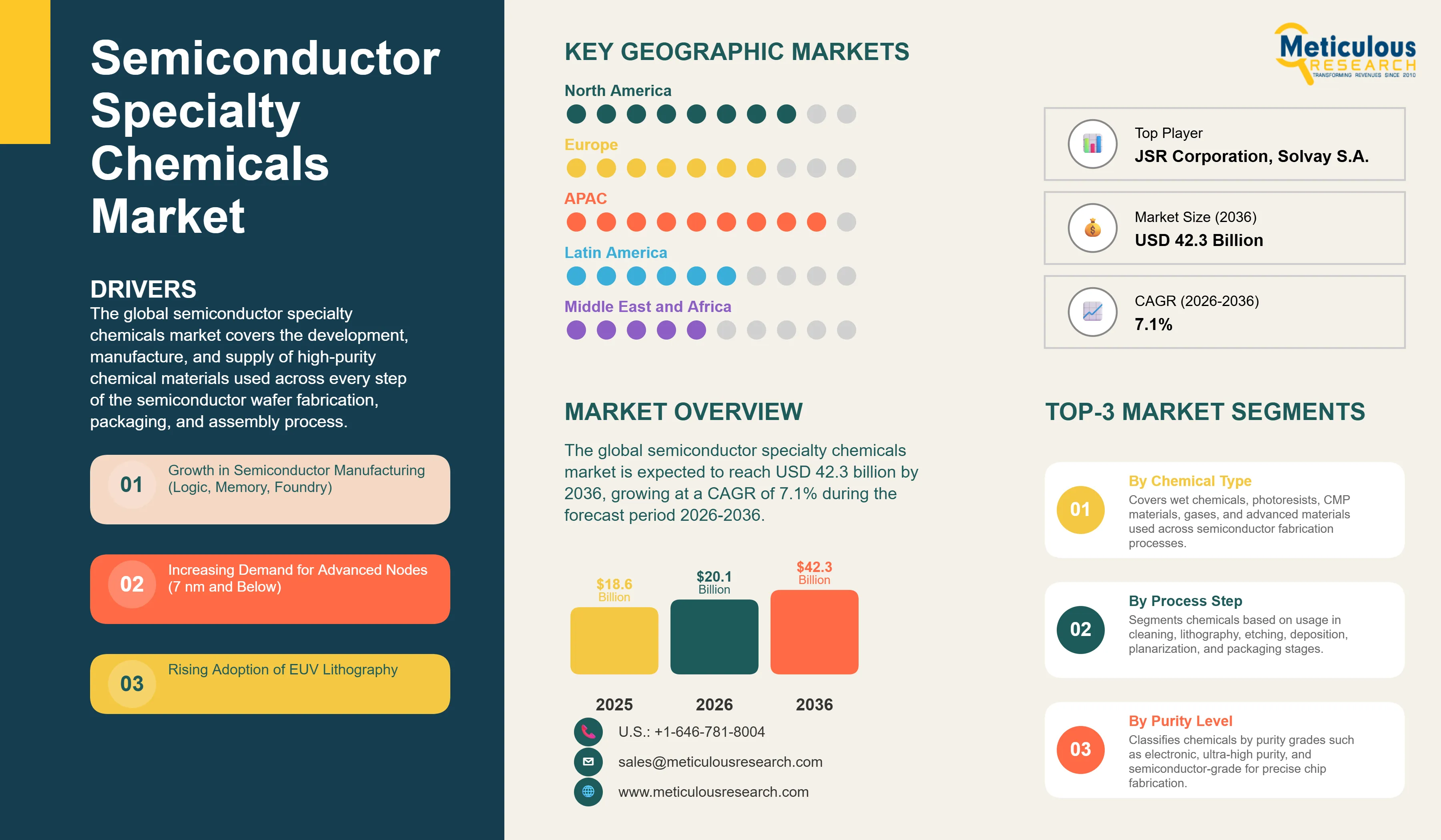
Report ID: MRCHM - 1041891 Pages: 340 Apr-2026 Formats*: PDF Category: Chemicals and Materials Delivery: 24 to 72 Hours Download Free Sample ReportThe global semiconductor specialty chemicals market was valued at USD 18.6 billion in 2025. This market is expected to reach USD 42.3 billion by 2036 from an estimated USD 20.1 billion in 2026, growing at a CAGR of 7.1% during the forecast period 2026-2036.
 Click here to: Get Free Sample Pages of this Report
The global semiconductor specialty chemicals market covers the development, manufacture, and supply of high-purity chemical materials used across every step of the semiconductor wafer fabrication, packaging, and assembly process. The market encompasses wet process chemicals including acids, solvents, and bases used for wafer cleaning and etching; photoresist formulations and ancillary chemicals including developers, strippers, and anti-reflective coatings used in lithographic patterning; chemical mechanical planarization slurries and consumables used for surface planarization; specialty gases and metal-organic precursors used in chemical vapor deposition and atomic layer deposition processes; and packaging chemicals used in advanced back-end assembly including underfill resins, die attach materials, and encapsulants. The market spans the full spectrum of semiconductor end users including integrated device manufacturers, pure-play foundries, and outsourced semiconductor assembly and test service providers.
The growth of the global semiconductor specialty chemicals market is primarily driven by the accelerating transition of leading semiconductor manufacturers toward sub-7 nm and sub-3 nm advanced process nodes that require substantially greater chemical consumption per wafer pass, higher purity specifications, and entirely new classes of specialty chemical formulations compared with legacy node manufacturing. Taiwan Semiconductor Manufacturing Company's progressive ramp of its N3 and N2 process generations, Samsung Foundry's 3 nm gate-all-around process, and Intel Foundry's 18A node development are each driving qualification and adoption of novel EUV photoresist chemistries, advanced precursor materials for gate-all-around transistor fabrication, and next-generation CMP slurry formulations capable of achieving the atomic-scale planarity specifications required at leading-edge nodes. The global surge in semiconductor fab investment, catalyzed by the U.S. CHIPS and Science Act, the European Chips Act, India's Semiconductor Mission, and Japan's Rapidus advanced node program, is expanding aggregate specialty chemical demand as new fab capacity across geographies comes online through the forecast period.
However, the market faces important structural constraints. The extreme purity requirements of leading-edge semiconductor processes, where metallic contaminant levels in process chemicals must be controlled to the sub-parts-per-trillion level to avoid yield loss and device reliability degradation, impose substantial research and development, production, and quality assurance investment requirements on specialty chemical suppliers that create high barriers to competitive entry and limit the supplier base for the most demanding purity tiers. The geographic concentration of both specialty chemical production and semiconductor manufacturing in a small number of countries, principally Japan, the United States, Germany, and Taiwan, creates supply chain concentration risk that has been highlighted by pandemic-era supply disruptions and is prompting both chemical producers and semiconductor manufacturers to invest in supply chain diversification strategies that require significant capital and time to execute.
Despite these challenges, the market outlook is strongly positive. The structural growth of semiconductor content in automotive electronics, artificial intelligence accelerator hardware, high-performance computing systems, and advanced communications infrastructure is sustaining above-trend semiconductor volume growth that translates directly into specialty chemical demand growth. The commercialization of extreme ultraviolet lithography at high-volume manufacturing scale by TSMC, Samsung, and Intel is opening a substantial new market opportunity for EUV-specific photoresist chemistries, EUV pellicle materials, and ancillary chemicals compatible with EUV process requirements that is creating high-value incremental revenue streams for specialty chemical suppliers with the technical capability to serve this demanding application.
|
Parameters |
Details |
|
Market Size by 2036 |
USD 42.3 Billion |
|
Market Size in 2026 |
USD 20.1 Billion |
|
Market Size in 2025 |
USD 18.6 Billion |
|
Revenue Growth Rate (2026-2036) |
CAGR of 7.1% |
|
Dominating Chemical Type |
Wet Chemicals |
|
Fastest Growing Chemical Type |
Photoresists and Ancillary Chemicals |
|
Dominating Process Step |
Lithography |
|
Fastest Growing Process Step |
Packaging and Assembly |
|
Dominating Purity Level |
Ultra-High Purity (UHP) Grade |
|
Fastest Growing Purity Level |
Semiconductor Grade (Sub-ppb/pptr) |
|
Dominating Technology Node |
7 nm to 14 nm |
|
Fastest Growing Technology Node |
3 nm and Below (Advanced Nodes) |
|
Dominating Application |
Foundry Services |
|
Fastest Growing Application |
Advanced Packaging (2.5D/3D IC) |
|
Dominating End User |
Foundries |
|
Fastest Growing End User |
OSAT |
|
Dominating Geography |
Asia-Pacific |
|
Fastest Growing Geography |
North America |
|
Base Year |
2025 |
|
Forecast Period |
2026 to 2036 |
Shift Toward Ultra-High Purity (UHP) Chemicals
The progressive tightening of metallic contamination specifications in semiconductor process chemicals across successive technology generations is the most pervasive structural trend in the semiconductor specialty chemicals market, as the shrinking feature dimensions and thinner gate dielectric layers of advanced node devices impose increasingly severe sensitivity to trace ionic and metallic impurities that can cause threshold voltage shifts, gate oxide degradation, and junction leakage at contamination levels that were inconsequential in larger geometry manufacturing. The transition from electronic grade to ultra-high purity grade and ultimately to the emerging semiconductor grade purity tier, where individual metallic contaminant concentrations must be controlled below the sub-parts-per-billion and in certain applications the sub-parts-per-trillion level, is requiring specialty chemical manufacturers to invest in dedicated high-purity production infrastructure, point-of-use purification systems, ultra-clean packaging technologies, and contamination-controlled logistics chains that substantially increase production complexity and cost but create defensible competitive positions for suppliers capable of achieving and maintaining the required purity performance.
Entegris has built a significant competitive position around UHP chemical supply and purification services, including its ATMI-acquired point-of-use purification systems and its specialty packaging and materials handling infrastructure. Merck KGaA's EMD Electronics division and Kanto Chemical's UHP wet chemistry product lines are advancing sub-ppb metallic purity specifications for acids and solvents used in gate oxide cleaning and post-etch residue removal at 3 nm and below node manufacturing. The increasing adoption of particle and metallic contamination monitoring within specialty chemical production lines, using inductively coupled plasma mass spectrometry and liquid particle counters, is enabling supplier quality systems to provide lot-level purity certification at the sub-ppb specification level required by leading-edge fab qualification requirements.
Increasing Demand for EUV Photoresists and Ancillaries
The high-volume manufacturing ramp of extreme ultraviolet lithography across TSMC, Samsung Foundry, and Intel Foundry is creating a rapidly expanding and technically demanding specialty chemical market for EUV-compatible photoresist formulations, EUV-specific anti-reflective coatings, and ancillary process chemicals whose performance requirements differ fundamentally from the chemically amplified DUV photoresist systems that dominated lithography chemistry for the preceding two decades. EUV photoresists must simultaneously achieve the high photon absorption at 13.5 nm wavelength, sub-20 nm line edge roughness, and stochastic defectivity performance required for patterning leading-edge logic and memory features at single-digit nanometer dimensions, while maintaining compatibility with the extreme cleanliness requirements of EUV scanner optics and pellicle systems. The development of metal oxide nanoparticle photoresist platforms, including those based on hafnium, tin, and zirconium-containing compounds, by Inpria (acquired by JSR Corporation), Merck KGaA, and DuPont represents a fundamentally new materials chemistry approach to EUV photoresist that is competing with advanced chemically amplified polymer photoresist formulations from Tokyo Ohka Kogyo, JSR, and Shin-Etsu Chemical for design-in positions at TSMC N2 and Samsung SF2 advanced nodes.
The EUV ancillary chemicals market, encompassing EUV-compatible developers, photoresist strippers, edge bead removers, and bottom anti-reflective coatings formulated for compatibility with the photon chemistry and etch selectivity requirements of EUV process flows, represents a high-value incremental revenue opportunity for established photoresist chemistry suppliers with the process integration knowledge and fab relationships required to qualify new ancillary formulations alongside their photoresist platforms. The anticipated transition to high-NA EUV lithography at sub-2 nm advanced nodes will impose even more stringent photoresist sensitivity, roughness, and stochastic performance requirements that are driving active next-generation photoresist development programs at all major photoresist suppliers.
Growth in Semiconductor Manufacturing (Logic, Memory, Foundry)
The sustained global expansion of semiconductor manufacturing capacity across logic, memory, and foundry segments represents the foundational structural driver of specialty chemical demand, as each silicon wafer processed through a semiconductor fabrication facility requires several hundred chemical process steps consuming measurable quantities of wet chemicals, photoresists, CMP slurries, specialty gases, and cleaning chemicals at each stage of the process flow. The ongoing capacity ramp at TSMC's Fab 21 in Arizona, Fab 18 in Taiwan, and its new Japan fab in Kumamoto, combined with Samsung Foundry's Taylor, Texas expansion and Intel Foundry's Ohio and Germany facilities, is adding several hundred thousand wafer starts per month of new advanced node capacity over the forecast period that will require commensurate specialty chemical supply. Memory manufacturers including SK Hynix, Micron, and Samsung are investing heavily in high-bandwidth memory capacity expansion to serve the insatiable memory bandwidth requirements of AI training and inference accelerator systems, driving memory specialty chemical consumption growth above historical trend rates. The strong demand for mature node capacity serving automotive, industrial, and microcontroller applications is supporting sustained chemical demand growth at legacy node fabs operated by United Microelectronics Corporation, GlobalFoundries, and multiple Chinese foundries.
Increasing Demand for Advanced Nodes (7 nm and Below)
The accelerating adoption of advanced process nodes at 7 nm and below by fabless semiconductor designers targeting artificial intelligence, high-performance computing, mobile application processor, and networking chip applications is creating disproportionately strong specialty chemical demand growth relative to overall wafer volume growth, as advanced node manufacturing processes require greater numbers of lithographic patterning steps per wafer, higher-purity chemical specifications for each process step, and entirely new categories of specialty chemicals for processes including EUV lithography, atomic layer deposition of high-k dielectrics and metal gate materials, and advanced packaging integration that do not exist in legacy node process flows. TSMC's 3 nm N3E process generation requires approximately 20% more EUV exposures per wafer than its predecessor N5 process, each requiring photoresist coat, develop, and strip chemical applications, substantially increasing photoresist and ancillary chemical consumption per wafer pass relative to DUV-only process nodes. The transition of the leading semiconductor node from fin field-effect transistor architecture to gate-all-around nanosheet transistor architecture at 3 nm and 2 nm node generations is requiring new precursor chemistries for selective deposition and selective etch process steps that have no direct precedent in established process chemical qualification libraries, creating significant development and qualification opportunities for specialty chemical suppliers with advanced precursor synthesis capabilities.
Growth of EUV Lithography Materials
The continuing high-volume manufacturing ramp of extreme ultraviolet lithography across leading-edge foundry and memory manufacturing, combined with the anticipated transition to high-NA EUV lithography systems at sub-2 nm node generations, represents the single most significant new market creation opportunity in the semiconductor specialty chemicals landscape over the forecast period. EUV lithography requires photoresist formulations, ancillary process chemicals, and pellicle materials that are entirely distinct from those used in deep ultraviolet lithography, creating a completely new materials chemistry market that did not exist at commercial scale a decade ago and is now growing rapidly as EUV layer counts per wafer increase with each successive technology node generation. The commercial opportunity for EUV-specific specialty chemicals is substantially larger than the photoresist unit volume alone, as each EUV exposure requires a complete chemical process sequence including anti-reflective coating deposition, photoresist coat, post-apply bake, exposure, post-exposure bake, development, inspection, and strip or etch, each requiring specialty chemical formulations qualified specifically for EUV process compatibility. The development of next-generation directed self-assembly materials, e-beam lithography resists, and nanoimprint lithography resins for sub-angstrom feature definition beyond the capability of even high-NA EUV represents a longer-term research-stage opportunity for specialty chemical suppliers investing in advanced patterning materials R&D.
Increasing Use of Advanced Packaging (2.5D/3D IC)
The structural adoption of advanced packaging architectures as the primary vehicle for continuing system-level performance scaling beyond the practical limits of front-end process node shrinking represents a significant and growing specialty chemical market opportunity that is expanding the addressable market of semiconductor specialty chemical suppliers beyond their traditional wafer fabrication focus. The adoption of TSMC CoWoS, InFO, and SoIC advanced packaging technologies by Apple, Nvidia, AMD, and Broadcom for their most demanding chip products is driving rapidly growing demand for specialty chemicals serving redistribution layer lithography, through-silicon via formation, hybrid bonding surface preparation, and precision underfill dispensing applications. Each 2.5D integrated circuit package incorporating a silicon interposer and multiple chiplets requires through-silicon via etching with specialized fluorine chemistry, electrochemical copper filling with plating chemistry, CMP planarization of copper via surfaces, and redistribution layer photolithography chemistry for each metal interconnect level, creating chemical consumption intensity per package that approaches the chemical consumption of the front-end wafer fabrication processes for the individual chiplets. The rapid growth of high-bandwidth memory for AI accelerator applications, which uses 3D DRAM die stacking with through-silicon via interconnects at the wafer level, is creating particularly strong demand for specialty chemicals serving memory-specific advanced packaging process requirements.
By Chemical Type: In 2026, Wet Chemicals to Dominate
Based on chemical type, the global semiconductor specialty chemicals market is segmented into wet chemicals (acids, solvents, and bases), photoresists and ancillary chemicals, CMP slurries, CMP pads and consumables, specialty gases and precursors, cleaning chemicals, and packaging chemicals. In 2026, the wet chemicals segment is expected to account for the largest share of the global semiconductor specialty chemicals market. The large share of this segment is attributed to wet chemicals' role as the most volumetrically consumed category of semiconductor specialty chemicals, with hydrofluoric acid, sulfuric acid, hydrogen peroxide, hydrochloric acid, ammonium hydroxide, and isopropyl alcohol consumed in very large quantities at every wet cleaning, etching, and surface preparation step throughout the front-end wafer fabrication process flow. The RCA wet clean process sequence, which uses hydrogen peroxide-based SC-1 and SC-2 cleaning solutions to remove organic contamination, particles, and metallic impurities from silicon wafer surfaces, is applied at dozens of process steps per wafer pass and represents the single largest wet chemical consumption application in semiconductor manufacturing. Leading wet chemical suppliers including Kanto Chemical, Stella Chemifa, and CMC Materials supply ultra-high purity acid and solvent products to fabs across Asia, North America, and Europe.
However, the photoresists and ancillary chemicals segment is poised to register the highest CAGR during the forecast period. The high growth of this segment is attributed to the rapid expansion of EUV lithography capacity at leading-edge fabs, the substantially higher per-wafer cost of EUV photoresist formulations relative to DUV photoresists, the increasing number of EUV layers per wafer at each successive advanced node generation, and the significant investment in next-generation photoresist development for high-NA EUV and beyond-EUV patterning applications that is creating a continuous innovation-driven revenue growth cycle in the photoresist category.
By Process Step: In 2026, Lithography to Hold the Largest Share
Based on process step, the global semiconductor specialty chemicals market is segmented into cleaning, lithography, etching, deposition, planarization (CMP), and packaging and assembly. In 2026, the lithography segment is expected to account for the largest share of the global semiconductor specialty chemicals market. This dominance reflects lithography's position as the most chemically intensive process step in terms of high-value specialty chemical consumption, encompassing photoresist materials, anti-reflective coating materials, immersion lithography topcoat chemistries, photoresist developers, and edge bead removal solvents that are applied and stripped at each of the dozens to over one hundred lithographic patterning steps per advanced node wafer. The high unit value of EUV photoresist formulations, which command price premiums of three to five times the cost of equivalent DUV photoresist materials per unit volume due to their technical complexity and limited supplier base, is maintaining the lithography step's dominant share of specialty chemical market value even as its volume share grows more modestly.
However, the packaging and assembly segment is projected to register the highest CAGR during the forecast period. This growth is driven by the structural adoption of advanced packaging architectures for AI accelerator, high-bandwidth memory, and high-performance computing applications that are substantially increasing back-end chemical consumption intensity, the premium pricing of advanced packaging specialty chemicals relative to legacy packaging materials, and the growing number of specialty chemical process steps in 2.5D and 3D integration package architectures that did not exist in traditional wire bond and flip-chip packaging.
By Purity Level: In 2026, Ultra-High Purity (UHP) Grade to Hold the Largest Share
Based on purity level, the global semiconductor specialty chemicals market is segmented into electronic grade, ultra-high purity (UHP) grade, and semiconductor grade (sub-ppb/pptr levels). In 2026, the ultra-high purity grade segment is expected to account for the largest share of the global semiconductor specialty chemicals market. This dominance reflects the broad adoption of UHP purity specifications across the mainstream of advanced node semiconductor manufacturing, where total metallic impurity concentrations in process chemicals must be controlled below the parts-per-billion level for the majority of cleaning, etching, and lithography applications at nodes of 14 nm and below. The UHP grade segment encompasses the largest installed base of chemical qualification programs and the broadest range of chemical product categories, spanning wet chemicals, photoresists, and cleaning formulations across the full population of advanced node fabs globally.
However, the semiconductor grade (sub-ppb/pptr) segment is projected to register the highest CAGR during the forecast period. This growth reflects the tightening of metallic contamination specifications at leading-edge nodes of 3 nm and below, where the highest-purity tier is becoming the required standard for gate oxide cleaning chemicals, EUV photoresist formulations, and atomic layer deposition precursors used in the most contamination-sensitive process steps of advanced transistor fabrication. This segment is critical for pricing differentiation, as sub-ppb/pptr grade chemicals command significant price premiums over standard UHP products due to the additional production and quality assurance investment required to achieve the most stringent purity specifications.
By Technology Node: In 2026, 7 nm to 14 nm to Hold the Largest Share
Based on technology node, the global semiconductor specialty chemicals market is segmented into 28 nm and above, 14 nm to 28 nm, 7 nm to 14 nm, 7 nm and below, and 3 nm and below (advanced nodes). In 2026, the 7 nm to 14 nm segment is expected to account for the largest share of the global semiconductor specialty chemicals market. This dominance reflects the concentration of high-volume production capacity at TSMC, Samsung, and GlobalFoundries in the 5 nm to 12 nm node range that represents the current production sweet spot for high-volume consumer chip, networking, and AI inference applications, combined with the high chemical intensity per wafer at these nodes relative to legacy 28 nm and above processes. The 7 nm to 14 nm node range encompasses multiple generations of EUV and DUV lithography-intensive process flows with the highest specialty chemical value per wafer of any currently mature production node generation.
However, the 3 nm and below advanced nodes segment is projected to register the highest CAGR during the forecast period. This growth is driven by the accelerating production ramp of TSMC's N3 and N2 process generations, Samsung's SF3 and SF2 gate-all-around processes, and Intel's 18A node, each of which requires the highest-purity and most technically advanced specialty chemical formulations currently in existence, commands the highest chemical cost per wafer of any process generation, and will progressively account for a growing share of global wafer starts through the forecast period as AI chip, mobile processor, and high-performance computing demand drives capacity investment at the leading edge.
By Application: In 2026, Foundry Services to Hold the Largest Share
Based on application, the global semiconductor specialty chemicals market is segmented into logic devices, memory (DRAM and NAND), foundry services, and advanced packaging (2.5D/3D IC). In 2026, the foundry services segment is expected to account for the largest share of the global semiconductor specialty chemicals market. This dominance reflects the concentration of leading-edge specialty chemical consumption in the pure-play foundry sector, where TSMC alone accounts for over 50% of global advanced logic foundry capacity and represents the single largest individual customer for EUV photoresists, advanced CMP slurries, and leading-edge wet process chemicals globally. The fabless semiconductor design model's structural growth, driven by the proliferation of AI chip startups, application processor developers, and networking chip designers that outsource manufacturing to foundries, is sustaining above-trend demand growth for foundry services and the specialty chemicals that support them.
However, the advanced packaging segment is projected to register the highest CAGR during the forecast period. This growth is driven by the structural adoption of 2.5D and 3D integration architectures across the highest-volume and highest-value semiconductor applications including AI accelerators, high-bandwidth memory, and high-performance computing processors, the premium specialty chemical cost intensity of advanced packaging processes relative to traditional packaging, and the rapidly expanding outsourced semiconductor assembly and test sector capacity investment to serve the growing advanced packaging demand from fabless customers and integrated device manufacturers.
By End User: In 2026, Foundries to Hold the Largest Share
Based on end user, the global semiconductor specialty chemicals market is segmented into integrated device manufacturers, foundries, and OSAT providers. In 2026, the foundries segment is expected to account for the largest share of the global semiconductor specialty chemicals market. This dominance reflects the foundry sector's concentration of the world's most advanced and chemically intensive semiconductor manufacturing processes, with TSMC, Samsung Foundry, GlobalFoundries, and United Microelectronics Corporation collectively operating the majority of global advanced and mature node wafer fabrication capacity that consumes the largest volume and highest value of specialty chemicals. The foundry business model, which serves a diverse ecosystem of fabless chip designers requiring custom process node access without captive manufacturing investment, has enabled foundries to invest in the most capital-intensive and chemically advanced process technologies that generate the highest specialty chemical demand intensity per wafer.
However, the OSAT segment is projected to register the highest CAGR during the forecast period. This growth reflects the rapid expansion of advanced packaging services by leading OSAT providers including ASE Technology, Amkor Technology, JCET, and Powertech Technology in response to the structural demand growth for 2.5D and 3D integration packaging, the increasing chemical process complexity and specialty chemical consumption intensity of advanced packaging relative to traditional wire bond services, and the strategic investment by OSAT providers in hybrid bonding, fan-out wafer-level packaging, and silicon photonics integration capabilities that require new categories of specialty chemicals not previously used in back-end semiconductor assembly.
Semiconductor Specialty Chemicals Market by Region: Asia-Pacific Leading by Share, North America by Growth
Based on geography, the global semiconductor specialty chemicals market is segmented into Asia-Pacific, North America, Europe, Latin America, and the Middle East and Africa.
In 2026, Asia-Pacific is expected to account for the largest share of the global semiconductor specialty chemicals market. The largest share of this region is mainly due to Asia-Pacific's overwhelming concentration of global semiconductor manufacturing capacity, with Taiwan, South Korea, Japan, and China collectively accounting for over 80% of global wafer fabrication output and representing the primary consumption geography for all categories of semiconductor specialty chemicals. TSMC's Taiwan fab complex, which includes the world's highest-volume and most technically advanced semiconductor manufacturing facilities, represents the single largest geographic concentration of advanced semiconductor specialty chemical consumption globally. South Korea's Samsung Electronics and SK Hynix are the world's two largest memory manufacturers and among the most significant consumers of CMP slurries, wet chemicals, and photoresists for DRAM and NAND flash production. Japan's dual role as both a major specialty chemical producer and a significant semiconductor manufacturer, with Sony's image sensor fabs, Kioxia's NAND flash facilities, and Renesas' automotive semiconductor manufacturing, creates a large domestic specialty chemical consumption base alongside the country's global export-oriented chemical supply infrastructure. China's semiconductor manufacturing sector, including SMIC, Hua Hong Semiconductor, and Yangtze Memory Technologies, represents a large and growing specialty chemical consumption market for mature and mid-range node processes, albeit one operating under technology access restrictions that are shaping the competitive dynamics of chemical supply to Chinese fabs.
However, North America is expected to grow at the fastest CAGR during the forecast period. The region's rapid growth is driven by the unprecedented wave of semiconductor fab investment in the United States enabled by the CHIPS and Science Act subsidy program, which is catalyzing the construction of TSMC Fab 21 in Arizona targeting N3 and N2 process production, Samsung's Taylor Texas facility targeting 4 nm and 2 nm production, Intel's Ohio campus targeting 18A and 14A advanced node manufacturing, and Micron's Idaho memory fab expansion targeting advanced DRAM production. Each of these facilities will require substantial specialty chemical supply at volumes and purity specifications that will drive significant North American specialty chemical demand growth well above historical regional trend rates as these fabs ramp to full production capacity through the 2026 to 2030 portion of the forecast period. The strategic positioning of U.S.-based specialty chemical suppliers including Entegris, Air Products, and Linde to serve the emerging U.S. fab cluster, combined with the establishment of U.S. production facilities by Japanese and European chemical suppliers seeking to maintain their supply relationships with their fab customers manufacturing in America, is building the North American specialty chemical supply infrastructure required to support the region's rapid fab capacity growth.
Europe represents a modest but strategically significant and growing regional market for semiconductor specialty chemicals, anchored by the region's specialty chemical production heritage in Germany, the Netherlands, and Belgium and the emerging advanced semiconductor manufacturing investments supported by the European Chips Act. ASML's EUV and deep ultraviolet lithography systems, manufactured in Eindhoven, Netherlands, are the global monopoly supply for advanced lithography equipment used by all leading semiconductor manufacturers and create a strategic European anchor in the semiconductor supply chain ecosystem that supports specialty chemical supplier relationships. The IMEC research institute in Leuven, Belgium serves as a global collaborative semiconductor research hub where leading specialty chemical suppliers evaluate next-generation chemical formulations in advanced process integration environments, providing European research infrastructure for process chemistry development that attracts chemical supplier R&D investment to the region.
The global semiconductor specialty chemicals market is characterized by a highly concentrated competitive structure dominated by a small number of established global suppliers with the ultra-high purity production infrastructure, process chemistry technical expertise, and semiconductor manufacturer qualification relationships required to serve the most demanding leading-edge fab requirements. The concentration reflects the substantial barriers to entry imposed by multi-year fab qualification timelines, the capital intensity of UHP production infrastructure, the depth of process integration knowledge required to develop chemicals compatible with increasingly complex fab process flows, and the risk aversion of semiconductor manufacturers who rely on stable, qualified chemical supply for yield-critical production operations. Competition is focused on purity performance, process compatibility, supply chain reliability, product innovation for next-generation process nodes, and geographic proximity to customer fabs rather than on commodity price competition that characterizes less technically demanding chemical markets.
The report provides a comprehensive competitive analysis based on an extensive assessment of leading players' technology platforms, product portfolios, geographic manufacturing footprint, customer qualification status, and key strategic developments. Key players operating in the global semiconductor specialty chemicals market include Entegris Inc. (U.S.), Merck KGaA / EMD Electronics (Germany), BASF SE (Germany), Kanto Chemical Co. Inc. (Japan), Tokyo Ohka Kogyo Co. Ltd. (Japan), JSR Corporation (Japan), Fujifilm Holdings Corporation (Japan), Shin-Etsu Chemical Co. Ltd. (Japan), Cabot Microelectronics / CMC Materials (U.S.), Air Products and Chemicals Inc. (U.S.), Linde plc (Ireland/U.K.), Versum Materials / Merck (U.S./Germany), Dow Inc. (U.S.), Solvay S.A. (Belgium), and DuPont de Nemours Inc. (U.S.), among others.
The global semiconductor specialty chemicals market is expected to reach USD 42.3 billion by 2036 from an estimated USD 20.1 billion in 2026, at a CAGR of 7.1% during the forecast period 2026-2036.
In 2026, the wet chemicals segment is expected to hold the largest share of the global semiconductor specialty chemicals market, driven by the extremely high volumetric consumption of acids, solvents, and base chemicals across wafer cleaning, etching, and surface preparation process steps that are applied at dozens of stages throughout the semiconductor fabrication process flow.
The photoresists and ancillary chemicals segment is expected to register the highest CAGR during the forecast period 2026-2036, driven by the rapid expansion of EUV lithography capacity at leading-edge fabs, the substantially higher unit value of EUV photoresist formulations relative to DUV photoresists, and the increasing number of EUV exposure layers per advanced node wafer that is creating compounding photoresist demand growth above overall wafer volume growth rates.
The semiconductor grade (sub-ppb/pptr levels) segment is the most critical for pricing differentiation and qualification positioning, as chemicals meeting sub-parts-per-billion metallic contamination specifications command the highest unit value premiums, serve the most technically demanding leading-edge node applications, and require the most extensive qualification investment from both suppliers and customers. This segment is projected to register the highest CAGR during the forecast period as 3 nm and below node manufacturing progressively requires the most stringent purity specifications across a broader range of chemical product categories.
The advanced packaging (2.5D/3D IC) segment is expected to register the highest CAGR during the forecast period, driven by the structural adoption of advanced packaging architectures for AI accelerator, high-bandwidth memory, and high-performance computing applications, the premium specialty chemical cost intensity of 2.5D and 3D integration processes relative to traditional packaging, and the rapidly expanding OSAT sector capacity investment in hybrid bonding, fan-out packaging, and silicon photonics integration capabilities.
The growth of this market is primarily driven by the sustained global expansion of semiconductor manufacturing capacity across logic, memory, and foundry segments, the accelerating transition to advanced nodes of 7 nm and below that require substantially greater chemical consumption intensity and higher purity specifications per wafer, the structural growth of AI, high-performance computing, and automotive electronics driving above-trend semiconductor demand, and the unprecedented wave of government-supported fab investment in the United States, European Union, Japan, and India that is creating new specialty chemical demand in previously underserved manufacturing geographies.
North America is expected to register the highest growth rate in the global semiconductor specialty chemicals market during the forecast period 2026-2036, driven by the unprecedented semiconductor fab investment wave catalyzed by the U.S. CHIPS and Science Act, including TSMC Fab 21 in Arizona, Samsung's Taylor Texas facility, Intel's Ohio campus, and Micron's Idaho memory expansion, which are collectively creating a new major U.S. semiconductor manufacturing cluster requiring specialty chemical supply at volumes that will drive North American market growth well above historical regional trend rates.
Key players are Entegris Inc. (U.S.), Merck KGaA / EMD Electronics (Germany), BASF SE (Germany), Kanto Chemical Co. Inc. (Japan), Tokyo Ohka Kogyo Co. Ltd. (Japan), JSR Corporation (Japan), Fujifilm Holdings Corporation (Japan), Shin-Etsu Chemical Co. Ltd. (Japan), Cabot Microelectronics / CMC Materials (U.S.), Air Products and Chemicals Inc. (U.S.), Linde plc (Ireland/U.K.), Versum Materials / Merck (U.S./Germany), Dow Inc. (U.S.), Solvay S.A. (Belgium), and DuPont de Nemours Inc. (U.S.), among others.
The primary yield-related challenge in semiconductor specialty chemical applications is the extreme sensitivity of advanced node manufacturing yield to trace metallic and particle contamination in process chemicals, where sub-parts-per-trillion levels of ionic or metallic impurities in gate oxide cleaning chemicals or lithography ancillaries can cause threshold voltage shifts, gate dielectric degradation, and junction leakage failures that reduce wafer-level yield. The asymmetric commercial risk this creates for specialty chemical suppliers, including potential financial liability for yield loss events and qualification suspension, is driving continuous investment in production infrastructure, analytical monitoring, and contamination exclusion systems that represent both a significant competitive differentiator for established UHP suppliers and a substantial barrier to competitive entry for new market participants.


Published Date: Feb-2026
Published Date: May-2022
Published Date: Jan-2024
Published Date: Feb-2025
Published Date: Feb-2026
Please enter your corporate email id here to view sample report.
Subscribe to get the latest industry updates