
Molecular Beam Epitaxy System Market (2026-2036)
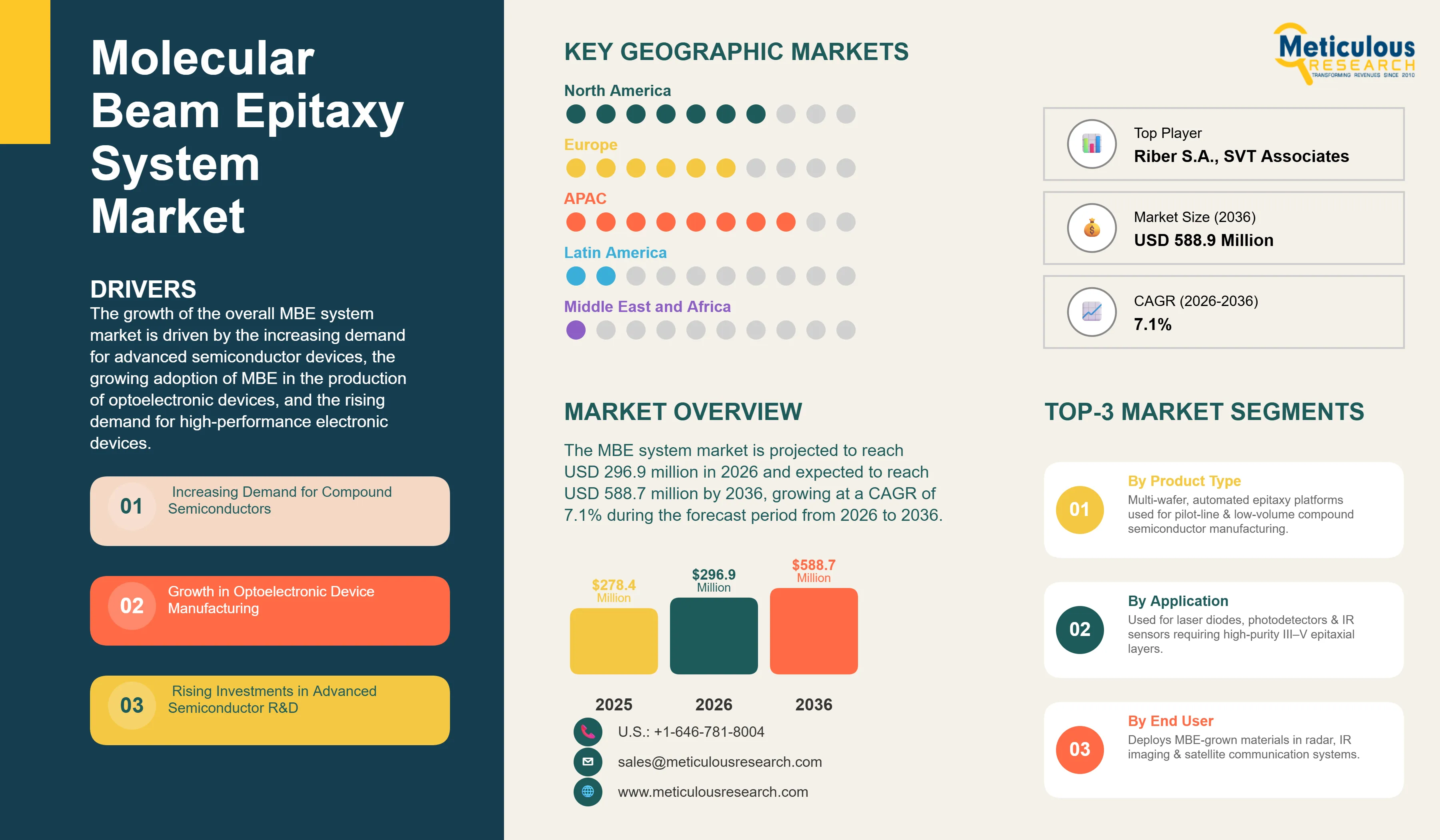
The global molecular beam epitaxy (MBE) system market is valued at USD 278.4 million in 2025 and is projected to reach USD 296.9 million in 2026. The market is further expected to reach USD 588.7 million by 2036, growing at a CAGR of 7.1% during the forecast period from 2026 to 2036.
- Published
- Feb 2026
- Pages
- 150
- Format
- PDF + Excel
- Report ID
- MR-297
- Base year
- 2025
- 2025 · BASELINE
- $278.4M
- 2036
- $588.7M
- CAGR 2026–2036
- 7.1%
2025 baseline · 2026–2036 forecast at 7.1% CAGR · hover a bar for the value
Key highlights
The global molecular beam epitaxy system market is projected to reach USD 588.7 million by 2036.
The market is expected to grow at a CAGR of 7.1% from 2026 to 2036.
The production MBE systems segment is expected to dominate the market in 2026, in terms of revenue.
The electronics industry is expected to be the largest end-user of MBE systems in 2026
North America is expected to command the largest share of the global MBE system market in 2026
Key players are focusing on technological advancements and strategic collaborations to enhance their market presence.
Report summary
| Particulars | Details |
|---|---|
| Market Size by 2036 | USD 588.7 Million |
| Market Size in 2026 | USD 296.9 Million |
| Revenue Growth Rate (2026-2036) | CAGR of 7.1% |
| Format | PDF, Excel & Cloud Portal · 150 pages |
| Dominating Product | Production MBE Systems |
| Leading End User | Electronics Industry |
| Leading Geographic Region | North America |
| Base Year | 2025 |
| Forecast Period | 2026 to 2036 |
Report overview
Segments covered: product, end user industry, epitaxy type, application.
The growth of the overall MBE system market is driven by the increasing demand for advanced semiconductor devices, the growing adoption of MBE in the production of optoelectronic devices, and the rising demand for high-performance electronic devices.
Molecular Beam Epitaxy (MBE) is a precision thin-film deposition technology used for the growth of ultra-high purity crystalline layers under ultra-high vacuum (UHV) conditions. The technique enables atomic-level control over material composition and thickness, making it critical for the fabrication of advanced compound semiconductor devices such as high-electron-mobility transistors (HEMTs), laser diodes, infrared detectors, and quantum well structures. MBE systems are widely utilized in the development of III–V semiconductor materials including gallium arsenide (GaAs), indium phosphide (InP), and gallium nitride (GaN), which are essential for high-frequency, high-power, and optoelectronic device applications.
The growing demand for advanced semiconductor components in telecommunications, aerospace & defense, and photonics is supporting increased investments in compound semiconductor fabrication technologies. For instance, according to the Semiconductor Industry Association (SIA), global semiconductor sales grew by over 19% in 2024, driven largely by demand for high-performance computing and wireless communication infrastructure. In addition, government-backed initiatives such as the U.S. CHIPS and Science Act and the European Union’s European Chips Act are encouraging investments in next-generation semiconductor R&D facilities, many of which incorporate MBE platforms for material innovation and device prototyping.
Market dynamics
3 factors across 3 forcesIncreasing Demand for Advanced Semiconductor Devices
The increasing demand for advanced compound semiconductor devices such as high-electron-mobility transistors (HEMTs), heterojunction bipolar transistors (HBTs), quantum cascade lasers (QCLs), and infrared photodetectors is a key factor driving the adoption of molecular beam epitaxy (MBE) systems. These devices are extensively utilized in high-frequency and high-power applications across wireless communication infrastructure, satellite systems, defense radar platforms, and optical sensing technologies.
For instance, GaAs- and InP-based RF components grown using epitaxial deposition technologies are widely used in 5G base stations and mobile communication modules to support high-frequency signal transmission. Additionally, MBE-grown III–V semiconductor layers are increasingly being used in advanced photonic integrated circuits (PICs) and infrared imaging systems deployed in aerospace & defense applications. As the demand for high-speed communication and precision sensing technologies continues to grow, semiconductor manufacturers and research institutions are increasing investments in epitaxial growth platforms to support next-generation device development, thereby driving demand for MBE systems.
Table of contents
11 chapters · 98 sections · 150 pages · click to expandSegmental analysis
| Segment | Largest share (2026) | Fastest growth (2026–2036) |
|---|---|---|
| By Product | Production MBE systems | — |
| By End-User | Electronics & semiconductor industry | — |
By Product
- Production MBE systems accounts for the largest share of the overall MBE system market in 2026, due to their increasing deployment in pilot-line and low-to-medium volume manufacturing environments for compound semiconductor devices.
- Unlike research-grade platforms, production MBE systems are equipped with multi-wafer handling capabilities, automated growth control, and in-situ monitoring technologies that enable improved process repeatability and material uniformity.
- These systems are primarily used in the fabrication of optoelectronic components such as laser diodes, photodetectors, and RF amplifiers that require high-purity epitaxial layers with precise compositional control.
- With growing demand for photonic devices in data communication, sensing, and defense electronics, semiconductor manufacturers are increasingly adopting production-scale MBE platforms to support industrial-grade epitaxial growth processes.
By End-User
- The electronics & semiconductor industry is expected to account for the largest share of the global MBE system market in 2026.
- This is primarily attributed to the increasing utilization of epitaxially grown III–V semiconductor materials in the development of RF communication devices, optoelectronic components, and advanced logic systems.
- In addition, research institutes and universities represent a significant end-user segment due to ongoing material science research related to quantum computing, spintronics, and nanophotonic devices.
- Government-funded semiconductor R&D initiatives across North America, Europe, and Asia-Pacific are supporting the deployment of compact and cluster-based MBE systems for material innovation and device prototyping.
Geographic analysis
Asia-Pacific
Largest shareAsia-Pacific is expected to account for the largest share of the global molecular beam epitaxy system market during the forecast period. This dominance is primarily attributed to the strong presence of semiconductor manufacturing hubs in countries such as China, Japan, South Korea, and Taiwan, along with increasing investments in compound semiconductor fabrication for telecommunications and consumer electronics applications. Furthermore, government-led semiconductor development programs across the region are supporting the establishment of advanced research facilities equipped with epitaxial growth platforms. For instance, national initiatives aimed at strengthening domestic semiconductor supply chains in China and South Korea are encouraging investments in next-generation material processing technologies, including MBE systems, for RF and photonic device applications.
North America
North America and Europe are also expected to witness steady growth, driven by increased funding for aerospace & defense electronics and quantum computing research, where precision epitaxial growth is critical for device performance.
Competitive landscape
- Veeco Instruments Inc.
- Riber S.A.
- DCA Instruments Oy
- SVT Associates, Inc.
- Dr. Eberl MBE-Komponenten GmbH
- SKY Technology Development Co., Ltd.
- Scienta Omicron GmbH
- SemiTEq JSC
- Pascal Co., Ltd.
- EIKO Engineering Co., Ltd.
Frequently asked questions
The global molecular beam epitaxy system market is valued at USD 296.9 million in 2026 and is expected to reach approximately USD 588.7 million by 2036.
Cite this report
Meticulous Research. (2026). Molecular Beam Epitaxy System Market - Global Opportunity Analysis and Industry Forecast (2026-2036) (Report No. MR-297). Meticulous Market Research Pvt. Ltd. https://www.meticulousresearch.com/product/molecular-beam-epitaxy-system-market-4998