Underfill Encapsulants Market (2026-2036)
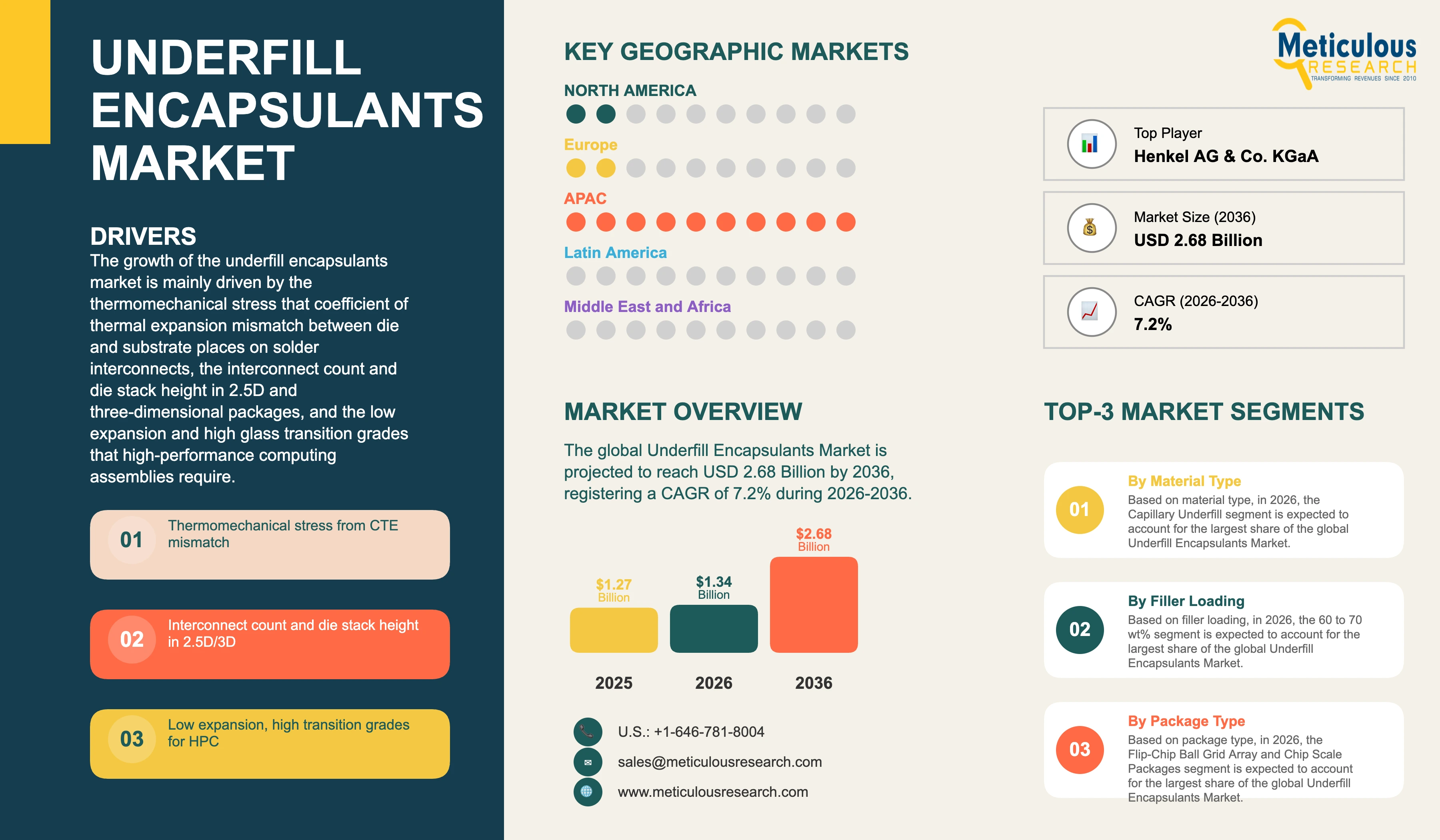
The global underfill encapsulants market was valued at USD 1.27 billion in 2025. This market is expected to reach USD 2.68 billion by 2036 from an estimated USD 1.34 billion in 2026, registering a CAGR of 7.2% during the forecast period (2026-2036).
- Published
- Nov 2026
- Pages
- 272
- Format
- PDF + Excel
- Report ID
- MRSE - 1042657
- Base year
- 2025
- 2025 · BASELINE
- $1.27B
- 2036
- $2.68B
- CAGR 2026–2036
- 7.2%
2025 baseline · 2026–2036 forecast at 7.2% CAGR · hover a bar for the value
Key highlights
The global underfill encapsulants market is estimated at USD 1.34 billion in 2026 and is projected to reach USD 2.68 billion by 2036.
Market volume is estimated at 18.60 kilotons in 2026 and is projected to reach 40.97 kilotons by 2036 at a CAGR of 8.2%.
The average selling price is estimated at USD 72.00 per kg in 2026 and is projected to reach USD 65.50 per kg by 2036.
Capillary underfill is expected to account for the largest material type share in 2026, while non-conductive film is projected to register the highest CAGR of 13.4%.
Filler loading of 60 to 70 wt% is expected to hold the largest share in 2026, while loading above 70 wt% is projected to grow fastest at a CAGR of 10.6%.
Flip-chip ball grid array and chip scale packages are expected to be the largest package type in 2026, while 2.5D and three-dimensional integrated packages are projected to register the highest CAGR of 14.2%.
Oven cure is expected to account for the largest cure process share in 2026, while thermocompression bonding cure is projected to grow fastest at a CAGR of 13.8%.
Smartphones and consumer electronics are expected to be the largest end-use application in 2026, while high-performance computing and data centre are projected to register the highest CAGR of 13.6%.
Asia-Pacific is expected to hold the largest regional share in 2026, while North America is projected to register the highest CAGR of 9.6%.
Commercial capillary underfill grades span filler loading from 50 to 72 wt%, with maximum filler particle size of 3 to 5 micrometres, according to Henkel AG & Co. KGaA product data.
Those grades carry glass transition temperatures from 90 to 135 degrees Celsius by thermomechanical analysis and 108 to 160 degrees Celsius by dynamic mechanical analysis.
Coefficient of thermal expansion below the glass transition ranges from 19 to 31 ppm per degree Celsius and above it from 62 to 120 ppm per degree Celsius across the same grades.
Viscosity across those capillary grades ranges from 4, 700 to 22,120 mPa s, and storage modulus at 25 degrees Celsius from 7 to 15 GPa.
Fracture toughness is reported from 1 to 3 MPa root metre, with the highest values on grades targeting advanced silicon nodes and 2.5D packages.
Capillary grades cure at 165 degrees Celsius for 2 hours with a 100 degrees Celsius hold, or at 150 degrees Celsius for 2 hours.
Non-conductive paste and film grades carry filler loading from 40 to 62 wt%, glass transition temperatures to 187 degrees Celsius by dynamic mechanical analysis, and stage life at 70 degrees Celsius of 40 to 120 minutes.
A non-conductive film grade for fine pitch bump protection is specified at 40 wt% filler with controlled flow and no resin bleed-out, curing at 175 degrees Celsius for 2 hours.
A liquid compression molding wafer-level encapsulant is specified with a 10 micrometre upper filler cut for gap and trench fill, in-mold cure at 120 degrees Celsius for 5 minutes and post-mold cure at 150 degrees Celsius for 1 hour.
That encapsulant is stated to deliver more than 70% warpage reduction, with glass transition temperature above 140 degrees Celsius, moisture sensitivity level 1, viscosity stability beyond 24 hours and a 12-month shelf life at minus 40 degrees Celsius.
Selected capillary underfill and wafer-level encapsulant grades are specified with no intentionally added PFAS, and the wafer-level grade is additionally stated as anhydride-free, REACH compliant and CMR-free.
Report summary
| Particulars | Details |
|---|---|
| Base Year | 2025 |
| Forecast Period | 2026-2036 |
| Market Size in 2025 | USD 1.27 billion |
| Market Size in 2026 | USD 1.34 billion |
| Market Size by 2036 | USD 2.68 billion |
| Value CAGR (2026-2036) | 7.2% |
| Format | PDF, Excel & Cloud Portal · 272 pages |
| Volume in 2026 | 18.60 kilotons |
| Volume by 2036 | 40.97 kilotons |
| Volume CAGR (2026-2036) | 8.2% |
| Average Selling Price in 2026 | USD 72.00 per kg |
| Average Selling Price by 2036 | USD 65.50 per kg |
| Measurement Basis | Capillary, no-flow, molded and wafer-level underfill together with non-conductive paste and film and liquid compression molding wafer-level encapsulant, excluding die attach adhesives, epoxy moulding compounds for standard package body encapsulation, glob top and dam-and-fill encapsulants for wire-bond assembly, conformal coatings, thermal interface materials, temporary bonding materials and hybrid bonding dielectrics |
| Largest Material Type Segment | Capillary underfill |
| Fastest-Growing Material Type Segment | Non-conductive film (CAGR 13.4%) |
| Largest Filler Loading Segment | 60 to 70 wt% |
| Fastest-Growing Filler Loading Segment | Above 70 wt% (CAGR 10.6%) |
| Largest Package Type | Flip-chip ball grid array and chip scale packages |
| Fastest-Growing Package Type | 2.5D and three-dimensional integrated packages (CAGR 14.2%) |
| Largest Cure Process | Oven cure |
| Fastest-Growing Cure Process | Thermocompression bonding cure (CAGR 13.8%) |
| Largest End-Use Application | Smartphones and consumer electronics |
| Fastest-Growing End-Use Application | High-performance computing and data centre (CAGR 13.6%) |
| Largest Region | Asia-Pacific |
| Fastest-Growing Region | North America (CAGR 9.6%) |
| Segments Covered | Material Type, Filler Loading, Package Type, Cure Process, End-Use Application, and Geography |
| Geographies Covered | Asia-Pacific, North America, Europe, Middle East & Africa, and Latin America |
| Companies Profiled | 10 companies, including Henkel AG & Co. KGaA, Namics Corporation, Resonac Holdings Corporation, Sumitomo Bakelite Co., Ltd., Panasonic Holdings Corporation, and Nagase & Co., Ltd. |
Report overview
Segments covered: material type, filler loading, package type, cure process, end-use application.
In volume terms, this market is estimated at 18.60 kilotons in 2026 and is projected to reach 40.97 kilotons by 2036, registering a CAGR of 8.2% during the same period. The average selling price is estimated at USD 72.00 per kg in 2026 and is projected to decline to USD 65.50 per kg by 2036 as capillary underfill moves from premium to mainstream flip-chip assembly and regional compounding capacity expands in Asia-Pacific.
The growth of this market is mainly driven by the thermomechanical stress on solder interconnects that coefficient of thermal expansion mismatch between die and substrate creates, the 2.5D and three-dimensional packages whose interconnect count and die stack height make underfill a structural element, the high-performance computing and data centre assemblies that require low coefficient of thermal expansion and high glass transition temperature grades, and the fine pitch bump protection that non-conductive film provides where capillary flow cannot reach. However, factors such as the capillary flow time that rises as bump pitch falls and gap height shrinks, and the displacement of non-conductive film by direct copper-to-copper hybrid bonding in the finest-pitch stacks, are expected to restrain the growth of this market to some extent.
Capillary underfill accounts for the largest share of this market because it serves the flip-chip ball grid array and chip scale packages that make up most flip-chip assembly and is dispensed at the highest volume per package. Non-conductive film grows faster because stacked die assembly applies the material before bonding rather than flowing it afterwards, which is the only route available at the bump pitches memory stacking now uses.
Underfill encapsulants are polymeric materials introduced into the gap between a flip-chip die and its substrate, or between stacked die, to redistribute the thermomechanical stress that would otherwise be carried by the solder interconnects alone. Market sizing in this report is on both a value basis in USD and a volume basis in kilotons, with average selling price derived from the two. The measurement basis is capillary, no-flow, molded and wafer-level underfill together with non-conductive paste and film and liquid compression molding wafer-level encapsulant, and it excludes die attach adhesives, epoxy moulding compounds used for standard package body encapsulation, glob top and dam-and-fill encapsulants for wire-bond assembly, conformal coatings, thermal interface materials, temporary bonding materials and hybrid bonding dielectrics.
Silicon expands at roughly a third of the rate of an organic substrate, so every thermal cycle strains the solder joints between them, and the strain concentrates at the die corners where the displacement is greatest. An underfill bonded to both surfaces couples them mechanically so that the polymer rather than the solder carries the differential movement, which is what converts a joint that would fail in hundreds of cycles into one that survives thousands. The material is therefore a reliability component rather than an assembly aid, and it is specified against the package rather than against the dispensing equipment.
Formulation is an exercise in balancing properties that move against each other. Commercial capillary grades span filler loading from 50 to 72 wt% with maximum particle size of 3 to 5 micrometres according to Henkel AG & Co. KGaA product data, and that loading sets both the coefficient of thermal expansion and the viscosity at once. Expansion below the glass transition ranges from 19 to 31 ppm per degree Celsius and above it from 62 to 120 ppm per degree Celsius, while viscosity across the same grades ranges from 4,700 to 22,120 mPa s. Raising filler content lowers the expansion that causes the problem and raises the viscosity that makes the material harder to introduce.
Glass transition temperature governs where those two expansion values apply. The same grades carry transitions from 90 to 135 degrees Celsius by thermomechanical analysis and 108 to 160 degrees Celsius by dynamic mechanical analysis, with storage modulus at 25 degrees Celsius from 7 to 15 GPa falling by one to two orders of magnitude at 250 degrees Celsius. A package operating above the transition sees the higher expansion figure and the lower modulus, so the grade has to be matched to the junction temperature the device actually reaches. High-performance assemblies consequently require the high transition and low expansion grades rather than the easier-flowing ones.
Fracture toughness is reported separately because the failure mode changes with package size. Values of 1 to 3 MPa root metre are reported across commercial grades, with the highest on those targeting advanced silicon nodes and 2.5D packages, where a large die on a large substrate stores more elastic energy and a crack initiated at a filler particle or a die corner can propagate. The same grades combine high toughness with high transition temperature and low expansion, which is the combination advanced packaging requires and the reason those grades sit at the top of the price range.
Where the material is introduced depends on what the interconnect pitch allows. Capillary underfill is dispensed at the die edge after reflow and drawn into the gap by capillary action, which works while the gap is large enough and the flow path short enough for the material to fill completely in an acceptable time. Non-conductive paste and film are applied to the die or wafer before bonding and cure during thermocompression bonding, which removes the flow requirement entirely. A film grade for fine pitch bump protection is specified at 40 wt% filler with controlled flow and no resin bleed-out, curing at 175 degrees Celsius for 2 hours.
Stage life rather than shelf life governs the non-conductive materials on the line. Paste and film grades carry filler loading from 40 to 62 wt%, transitions to 187 degrees Celsius by dynamic mechanical analysis, and stage life at 70 degrees Celsius of 40 to 120 minutes, which is the window between application and bonding during which the material remains workable. A short window constrains how many die can be processed per batch and how a line recovers from a stoppage. Fluxing versions remove the separate flux step on copper organic solderability preservative finishes, and grades are qualified against specific surface finishes including tin and nickel gold.
Wafer-level encapsulation addresses warpage rather than interconnect stress. A liquid compression molding grade is specified with a 10 micrometre upper filler cut for gap and trench fill, in-mold cure at 120 degrees Celsius for 5 minutes followed by post-mold cure at 150 degrees Celsius for 1 hour, and is stated to deliver more than 70% warpage reduction with a transition above 140 degrees Celsius, moisture sensitivity level 1, viscosity stability beyond 24 hours and a 12-month shelf life at minus 40 degrees Celsius. Fan-in and fan-out wafer level packaging and panel level packaging all depend on controlling warpage across the reconstituted substrate before the redistribution layers are built.
Formulation is also being constrained by substance content. Selected capillary underfill and wafer-level encapsulant grades are specified with no intentionally added PFAS, and the wafer-level grade is additionally stated as anhydride-free, REACH compliant and CMR-free. Those statements appear alongside the thermomechanical data rather than in separate documentation, which indicates that customers are selecting on substance content as well as on performance. Reformulating to remove a fluorinated surfactant or an anhydride hardener changes flow behaviour and cure profile, so the substitution is requalified rather than swapped.
Flip-chip ball grid array and chip scale packages are expected to account for the largest share in 2026.
2.5D and three-dimensional integrated packages are projected to register the highest CAGR of 14.2% during the forecast period.
Oven cure is expected to hold the largest share in 2026, reflecting the capillary grades curing at 165 degrees Celsius for 2 hours or 150 degrees Celsius for 2 hours.
Thermocompression bonding cure is projected to register the highest CAGR of 13.8% during the forecast period.
Smartphones and consumer electronics are expected to hold the largest share in 2026.
High-performance computing and data centre are projected to register the highest CAGR of 13.6% during the forecast period.
Asia-Pacific is expected to account for the largest share in 2026, supported by the concentration of semiconductor assembly, packaging and test capacity in Taiwan, South Korea, China, Japan, Malaysia and the Philippines. Taiwan is projected to grow at 7.4% and South Korea at 8.2%.
North America is projected to register the highest CAGR of 9.6% during the forecast period, with the United States at 9.8%.
Europe is projected to grow at a CAGR of 7.0%, with Germany at 7.2%. The regional position rests on automotive and industrial semiconductor assembly rather than high-volume consumer packaging, which concentrates demand on automotive-qualified grades carrying wider temperature ranges and longer thermal cycle counts.
The Middle East & Africa is projected to grow at a CAGR of 8.0% and Latin America at a CAGR of 5.0%, both from very small bases where board assembly rather than semiconductor packaging accounts for the activity.
Henkel AG & Co. KGaA, Namics Corporation, Resonac Holdings Corporation, Sumitomo Bakelite Co., Ltd. and Panasonic Holdings Corporation together accounted for an estimated 63.8% of this market in 2026. The 10 companies profiled in this report together accounted for an estimated 88.0%.
Report infographic
Market dynamics
15 factors across 5 forcesThermomechanical Stress from Coefficient of Thermal Expansion Mismatch
Silicon expands at roughly a third of the rate of an organic substrate, so each thermal cycle strains the solder interconnects between them and the strain concentrates at the die corners. An underfill bonded to both surfaces transfers that differential movement into the polymer, and commercial grades deliver expansion below the glass transition of 19 to 31 ppm per degree Celsius against the far higher figures above it, with storage modulus at 25 degrees Celsius from 7 to 15 GPa providing the stiffness that couples the two surfaces. Without the material the joints fail in thermal cycling long before the device reaches its service life. Underfill is therefore a condition of qualification for flip-chip packages rather than an option within the assembly process. The requirement also tightens as die grow, since the corner displacement that drives the failure scales with distance from the die centre.
Interconnect Count and Die Stack Height in 2.5D and Three-Dimensional Packages
A 2.5D package places large logic and memory die side by side on an interposer and a three-dimensional stack places die on top of one another, which multiplies the interconnect count and the stored elastic energy in the assembly. Grades targeting advanced silicon nodes and 2.5D packages carry fracture toughness of 3 MPa root metre against 1 MPa root metre on simpler chip-on-wafer grades, because a crack initiated at a die corner in a large assembly can propagate rather than arrest. Each bonded interface in a stack requires its own underfill or non-conductive film layer, so material consumption rises with stack height rather than with die count. Each interface is also qualified separately, since the thermal history of a lower layer in a stack differs from an upper one. The packages carry the highest value per unit, which supports the premium grades.
Low Expansion and High Transition Grades Required by High-Performance Computing
A high-performance computing or data centre device operates at a junction temperature that can exceed the glass transition of a general-purpose underfill, at which point the material shows the higher expansion figure of 62 to 120 ppm per degree Celsius and a storage modulus one to two orders of magnitude below its room-temperature value. Grades carrying transitions of 135 degrees Celsius by thermomechanical analysis and 160 degrees Celsius by dynamic mechanical analysis with expansion of 19 ppm per degree Celsius are formulated for those conditions at 72 wt% filler loading. The higher loading raises viscosity to the point where flow becomes the limiting factor, which is why these grades are developed alongside the dispensing process. Demand concentrates on the narrow set of grades holding all three properties at once, and those grades are developed against a specific package rather than offered from a catalogue.
Fine Pitch Bump Protection Where Capillary Flow Cannot Reach
Capillary underfill depends on a gap large enough and a flow path short enough for the material to fill completely, and both conditions deteriorate as bump pitch falls and die size rises. Non-conductive paste and film are applied before bonding and cure during thermocompression bonding, which removes the flow requirement entirely, and a film grade for fine pitch is specified at 40 wt% filler with controlled flow and no resin bleed-out. Resin bleed-out onto bond pads is what disqualifies a material in those applications rather than insufficient strength. The transition to pre-applied materials is consequently driven by geometry rather than by performance preference, which makes it durable. Applying the material at wafer level rather than at the assembly line also moves it earlier in the supply chain, changing who specifies and who dispenses it.
Table of contents
13 chapters · 136 sections · 272 pages · click to expandSegmental analysis
| Segment | Largest share (2026) | Fastest growth (2026–2036) |
|---|---|---|
| By Material Type | Capillary underfill | — |
| Other segments | — | Non-conductive film |
By Material Type
- Capillary underfill is expected to account for the largest share in 2026, serving the flip-chip ball grid array and chip scale packages that make up most flip-chip assembly.
- Filler loading of 60 to 70 wt% is expected to hold the largest share in 2026, balancing expansion control against the viscosity that allows capillary flow.
Other segments
- Non-conductive film is projected to register the highest CAGR of 13.4% during the forecast period.
- Loading above 70 wt% is projected to register the highest CAGR of 10.6% during the forecast period.
Geographic analysis
Asia-Pacific
Largest shareIn 2026, Asia-Pacific is expected to account for the largest share of the global underfill encapsulants market. The large share of this region is mainly due to the concentration of semiconductor assembly, packaging and test capacity in Taiwan, South Korea, China, Japan, Malaysia and the Philippines, the advanced packaging lines in Taiwan and South Korea that build 2.5D and stacked memory constructions, and the presence of the Japanese electronic materials suppliers that formulate most of the qualified grades. Taiwan is projected to register a CAGR of 7.4% and South Korea a CAGR of 8.2% during the forecast period.
North America
Fastest growthHowever, North America is projected to register the highest CAGR of 9.6% during the forecast period. The rapid growth of this region is attributed to the advanced packaging capacity being established alongside new front-end fabs in the United States, the high-performance computing and data centre devices designed there that require the high transition and low expansion grades, and the 2.5D interposer assembly those devices use. The United States is projected to register a CAGR of 9.8% during the forecast period.
Europe
Europe holds a smaller share concentrated in automotive and industrial semiconductor assembly rather than in high-volume consumer packaging, and is projected to grow at 7.0%, with Germany at 7.2%. Automotive-grade packages impose wider temperature ranges and longer thermal cycle counts than consumer packages on the same material class, which concentrates European demand on the automotive-qualified grades.
Middle East & Africa
The Middle East & Africa is projected to grow at 8.0% and Latin America at 5.0%, both from very small bases where board assembly rather than semiconductor packaging accounts for the activity. Formulation and consumption sit in different places in this market, and the qualification follows the package rather than the plant. Grades are developed by a small number of suppliers in Japan, Germany and the United States and qualified by the device owner against a specific package, junction temperature and reliability standard, so an assembly site in any region can run a qualified grade without repeating that work. Material is shipped in small, high-value quantities that bear freight comfortably, and several grades require cold storage, with one wafer-level encapsulant specified at minus 40 degrees Celsius for its 12-month shelf life. Cold chain and local technical support at the dispenser therefore matter more than regional compounding capacity, and a supplier without cold chain cannot serve the grades that need it however well they perform, which concentrates supply among the established distributors in each packaging centre.
Competitive landscape
The global underfill encapsulants market is characterised by the presence of diversified adhesives and electronic materials companies, Japanese specialty chemical groups with epoxy moulding compound and film positions, and specialist semiconductor encapsulant formulators. Competition is contested on qualified position in a specific package at a specific junction temperature rather than on formulation, since an underfill is validated through thermal cycling, moisture sensitivity and high-temperature storage testing as part of the package. Henkel AG & Co. KGaA, Namics Corporation, Resonac Holdings Corporation, Sumitomo Bakelite Co., Ltd. and Panasonic Holdings Corporation together accounted for an estimated 63.8% of this market in 2026, while the companies profiled in this report together accounted for an estimated 88.0%.
Product data is now published with filler loading, maximum particle size, glass transition by both thermomechanical and dynamic mechanical analysis, expansion above and below that transition, storage modulus at 25 and 250 degrees Celsius, fracture toughness and cure schedule together, which makes the formulation trade-offs directly comparable across suppliers. Selected grades are specified with no intentionally added PFAS and, for wafer-level encapsulation, as anhydride-free, REACH compliant and CMR-free. High toughness low expansion grades for 2.5D assembly, liquid compression molding encapsulants for wafer and panel level warpage control, and fluxing non-conductive pastes accounted for most competitive activity through 2026, alongside grades qualified specifically for automotive temperature competitive activity through 2026, alongside grades qualified specifically for automotive temperature ranges and cycle counts, which do not transfer from consumer qualifications.
The Japanese materials companies hold positions built on adjacent epoxy moulding compound, film and die attach capability in the same assembly operations, which gives them a qualification route that a single-product supplier does not have. Namics Corporation supplies semiconductor encapsulants as a principal business, while Element Solutions Inc and Nagase & Co., Ltd. compete through broader assembly materials portfolios. Some of the key players operating in the underfill encapsulants market are Henkel AG & Co. KGaA (Germany), Namics Corporation (Japan), Resonac Holdings Corporation (Japan), Sumitomo Bakelite Co., Ltd. (Japan), Panasonic Holdings Corporation (Japan), Nagase & Co., Ltd. (Japan), Element Solutions Inc (U.S.), Shin-Etsu Chemical Co., Ltd. (Japan), Kyocera Corporation (Japan), and Nitto Denko Corporation (Japan), among others.
- —
Capillary underfill grades have been brought to market at 72 wt% filler loading with expansion of 19 ppm per degree Celsius, glass transition of 160 degrees Celsius by dynamic mechanical analysis and fracture toughness of 3 MPa root metre for advanced silicon nodes and 2.5D packages. A liquid compression molding wafer-level encapsulant has been introduced with a 10 micrometre upper filler cut, in-mold cure at 120 degrees Celsius for 5 minutes and more than 70% warpage reduction. Selected grades are specified with no intentionally added PFAS and as anhydride-free, REACH compliant and CMR-free.
- Henkel AG & Co. KGaA
- Namics Corporation
- Resonac Holdings Corporation
- Sumitomo Bakelite Co., Ltd.
- Panasonic Holdings Corporation
- Nagase & Co., Ltd
Expert perspectives
Volume grows at 8.2% against 7.2% in value over the forecast period, and the average selling price falls from USD 72.00 per kg in 2026 to USD 65.50 per kg by 2036 as capillary underfill moves from premium to mainstream flip-chip assembly and regional compounding capacity expands in Asia-Pacific. The decline reflects a mix shift toward higher-volume packages rather than erosion of the premium on advanced grades, which holds wherever the junction temperature sits above a general-purpose glass transition.
Everything in this market reduces to one trade-off. Filler loading sets the coefficient of thermal expansion and the viscosity at the same time, and commercial grades span 4,700 mPa s at 50 wt% with 31 ppm per degree Celsius expansion to 11,930 mPa s at 72 wt% with 19 ppm per degree Celsius. Lowering the expansion the material exists to control makes it harder to introduce, which is why portfolios stay wide rather than converging and why each new package geometry reopens the balance.
Glass transition temperature rather than strength decides whether a grade qualifies. Expansion rises from the high teens or twenties to between 62 and 120 ppm per degree Celsius above the transition, and storage modulus falls by one to two orders of magnitude, so a package running above its underfill transition is operating with a different material than the one specified. That is the mechanism behind high-performance computing growing at 13.6% while consumer assembly carries the volume.
Fracture toughness is the property that separates advanced from mainstream grades. Values run from 1 MPa root metre on chip-on-wafer grades to 3 MPa root metre on grades for advanced nodes and 2.5D packages, because a large die on a large substrate stores elastic energy that a brittle underfill releases as a crack. Holding 3 MPa root metre together with 19 ppm per degree Celsius expansion and a 160 degrees Celsius transition is what narrows the qualified set at the top of this market.
The fastest-growing material type faces the clearest ceiling. Non-conductive film grows at 13.4% because pre-application removes the capillary flow requirement at pitches where flow fails, but a hybrid bonded interface has no polymer in the joint at all and is being adopted at exactly those finest pitches. Film therefore grows into a window that hybrid bonding closes from one end, and it holds the stacks where bump interconnects remain.
Wafer-level encapsulation is a different business inside the same market. A liquid compression molding grade addresses warpage across a reconstituted substrate rather than interconnect stress, is applied across the whole area rather than at die edges, and delivers more than 70% warpage reduction with in-mold cure in 5 minutes. Consumption per unit area is far higher than capillary underfill, which is why the segment matters more to volume than its package share suggests.
Customer perspectives
Junction temperature against glass transition rather than nominal expansion governs grade selection, and fracture toughness is the decisive property on large interposer assemblies.
Capillary fill time and the expansion penalty of thinning the material together drive the move to pre-applied films on fine pitch stacked assemblies rather than any performance advantage.
Automotive temperature ranges and cycle counts prevent transfer of consumer qualifications, and substance declarations on formulation content have become part of the materials selection alongside performance.
“The first question we ask is where our junction temperature sits relative to the glass transition. Above it the expansion and the modulus are different numbers entirely, so a grade that looks fine on paper is not the material our package actually runs on. For our large interposer parts we are also looking hard at fracture toughness, because a crack at a die corner is what we see fail.”
“As the pitch comes down, capillary fill time goes up and incomplete fill becomes a yield problem, not a cosmetic one. We can thin the material to recover flow but then the expansion goes the wrong way. On the fine pitch stacked parts we have stopped trying and moved to a film applied before bonding.”
“Our temperature range and cycle counts are wider than a consumer part, so a grade qualified for a phone does not carry over to us and we requalify from scratch. We are also now asking what is in the formulation, because declarations on fluorinated additives and hardeners follow the part into every market we ship to.”
Frequently asked questions
This market was valued at USD 1.20 billion in 2024 and USD 1.27 billion in 2025, and is estimated at USD 1.34 billion in 2026. In volume terms it is estimated at 18.60 kilotons in 2026.
Cite this report
Meticulous Research. (2026). Underfill Encapsulants Market - Global Opportunity Analysis and Industry Forecast (2026-2036) (Report No. MRSE - 1042657). Meticulous Market Research Pvt. Ltd. https://www.meticulousresearch.com/product/underfill-encapsulants-market-7340