Temporary Bonding Adhesives Market (2026-2036)
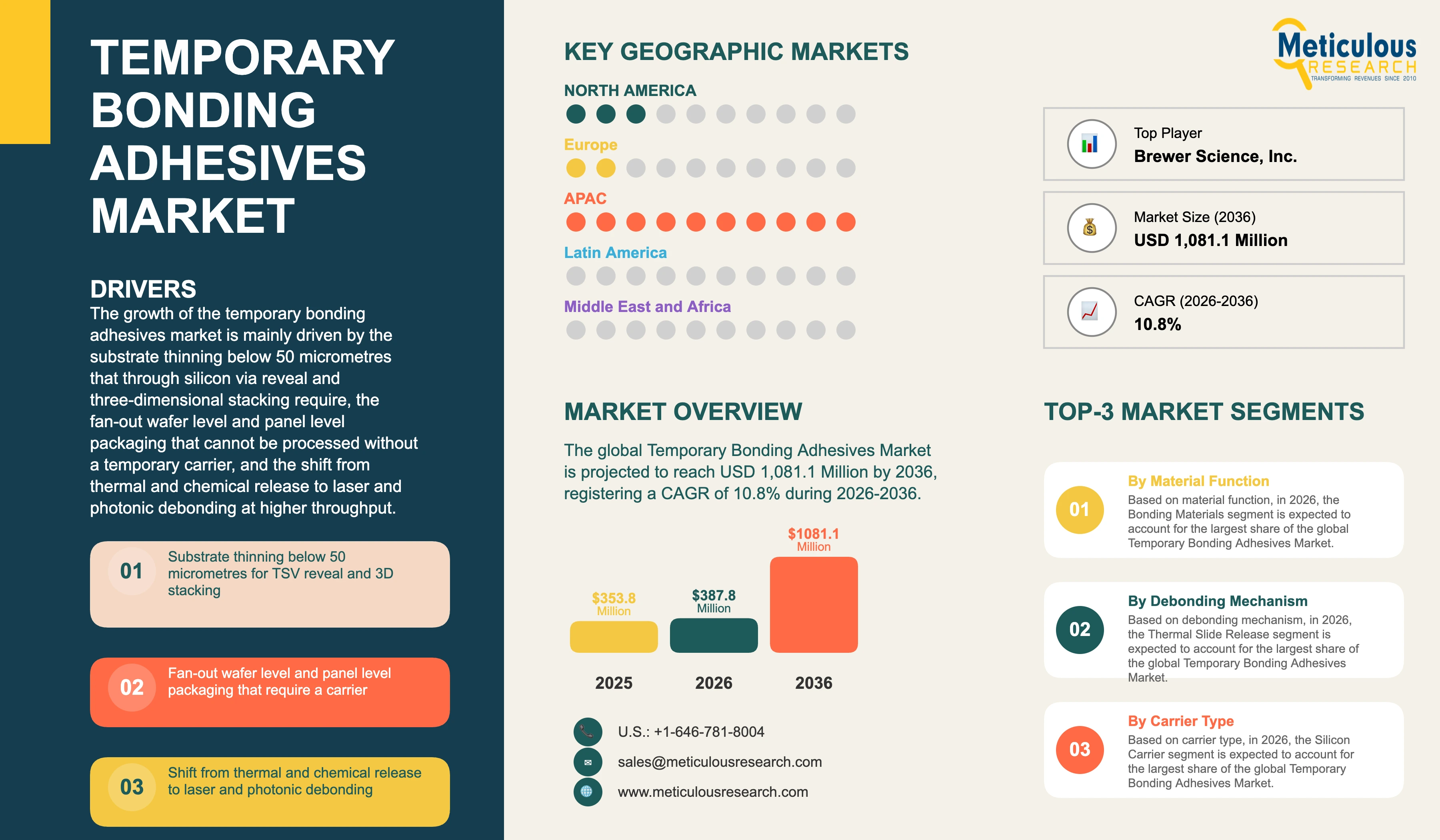
The global temporary bonding adhesives market was valued at USD 353.8 million in 2025. This market is expected to reach USD 1,081.1 million by 2036 from an estimated USD 387.8 million in 2026, registering a CAGR of 10.8% during the forecast period (2026-2036).
- Published
- Nov 2026
- Pages
- 257
- Format
- PDF + Excel
- Report ID
- MRSE - 1042656
- Base year
- 2025
- 2025 · BASELINE
- $353.8M
- 2036
- $1.08B
- CAGR 2026–2036
- 10.8%
2025 baseline · 2026–2036 forecast at 10.8% CAGR · hover a bar for the value
Key highlights
The global temporary bonding adhesives market is estimated at USD 387.8 million in 2026 and is projected to reach USD 1,081.1 million by 2036.
Market volume is estimated at 1.48 kilotons in 2026 and is projected to reach 4.68 kilotons by 2036 at a CAGR of 12.2%.
The average selling price is estimated at USD 262.00 per kg in 2026 and is projected to reach USD 231.00 per kg by 2036.
Bonding materials are expected to account for the largest material function share in 2026, while release layers are projected to register the highest CAGR of 14.8%.
Thermal slide release is expected to hold the largest share by debonding mechanism in 2026, while laser release is projected to grow fastest at a CAGR of 16.4%.
Silicon carriers are expected to account for the largest carrier type share in 2026, while glass carriers are projected to register the highest CAGR of 15.2%.
The 300 mm wafer format is expected to hold the largest substrate format share in 2026, while panel format is projected to grow fastest at a CAGR of 17.8%.
Wafer thinning and through silicon via reveal are expected to be the largest application in 2026, while fan-out wafer level packaging is projected to register the highest CAGR of 14.2%.
Asia-Pacific is expected to hold the largest regional share in 2026, while North America is projected to register the highest CAGR of 12.6%.
Temporary bonding platform requirements include substrate thinning to 50 micrometres or below and thermal stability to 400 degrees Celsius, according to Brewer Science, Inc.
Those requirements also include chemical resistance to photolithographic solutions, metal etch chemistries and general cleaning solvents, and compatibility with metals, epoxy moulding compounds and polyimides.
Five debonding mechanisms are in commercial use, namely chemical release, thermal slide release, mechanical release, laser release and photonic debonding.
Chemical release separates the device wafer from a perforated carrier in a solvent bath as a batch process running 25 wafers per cycle, with thermal stability to 220 degrees Celsius.
Thermal slide release separates the pair by heating and sliding the wafers apart at 15 wafers per hour, with thermal stability to 250 degrees Celsius.
Mechanical release uses a release material on the carrier at room temperature, running 20 wafers per hour with thermal stability to 400 degrees Celsius.
Laser release bonds the device wafer to a transparent glass carrier and exposes the release material through it, running 50 wafers per hour with thermal stability to 400 degrees Celsius, and is described as the lowest-stress option.
Photonic debonding uses a pulsed broadband light source with an inorganic light-absorbing layer on the carrier, running above 50 wafers per hour with thermal stability to 280 degrees Celsius.
Photonic debonding is stated as compatible with thinned device wafers below 20 micrometres and as tolerating slight bow or warp.
The stress the bonding layer has to survive arises from thermal cycling, coefficient of thermal expansion mismatch, mechanical grinding and metal deposition.
Report summary
| Particulars | Details |
|---|---|
| Base Year | 2025 |
| Forecast Period | 2026-2036 |
| Market Size in 2025 | USD 353.8 million |
| Market Size in 2026 | USD 387.8 million |
| Market Size by 2036 | USD 1,081.1 million |
| Value CAGR (2026-2036) | 10.8% |
| Volume in 2026 | 1.48 kilotons |
| Volume by 2036 | 4.68 kilotons |
| Volume CAGR (2026-2036) | 12.2% |
| Average Selling Price in 2026 | USD 262.00 per kg |
| Average Selling Price by 2036 | USD 231.00 per kg |
| Measurement Basis | Bonding materials and release layers consumed in temporary carrier flows, including the portion consumed in die-to-wafer hybrid bonding carrier flows, excluding permanent bonding and dielectric materials, dicing and backgrinding tapes, silicon and glass carriers themselves, third-party inorganic light-absorbing layers, and bonders, debonders and laser or photonic release equipment |
| Largest Material Function Segment | Bonding materials |
| Fastest-Growing Material Function Segment | Release layers (CAGR 14.8%) |
| Largest Debonding Mechanism | Thermal slide release |
| Fastest-Growing Debonding Mechanism | Laser release (CAGR 16.4%) |
| Largest Carrier Type | Silicon carrier |
| Fastest-Growing Carrier Type | Glass carrier (CAGR 15.2%) |
| Largest Substrate Format | 300 mm wafer |
| Fastest-Growing Substrate Format | Panel format (CAGR 17.8%) |
| Largest Application | Wafer thinning and through silicon via reveal |
| Fastest-Growing Application | Fan-out wafer level packaging (CAGR 14.2%) |
| Largest Region | Asia-Pacific |
| Fastest-Growing Region | North America (CAGR 12.6%) |
| Segments Covered | Material Function, Debonding Mechanism, Carrier Type, Substrate Format, Application, and Geography |
| Geographies Covered | Asia-Pacific, North America, Europe, Middle East & Africa, and Latin America |
| Companies Profiled | 10 companies, including Brewer Science, Inc., Tokyo Ohka Kogyo Co., Ltd., 3M Company, Nissan Chemical Corporation, Shin-Etsu Chemical Co., Ltd., and JSR Corporation |
Report overview
Segments covered: material function, debonding mechanism, carrier type, substrate format, application.
In volume terms, this market is estimated at 1.48 kilotons in 2026 and is projected to reach 4.68 kilotons by 2036, registering a CAGR of 12.2% during the same period. The average selling price is estimated at USD 262.00 per kg in 2026 and is projected to decline to USD 231.00 per kg by 2036 as materials move from qualification quantities into production supply and spin-coated layers are applied at lower thickness on larger substrate formats.
The growth of this market is mainly driven by the substrate thinning below 50 micrometres that through silicon via reveal and three-dimensional stacking require, the fan-out wafer level and panel level packaging that cannot be processed without a temporary carrier, the shift from thermal and chemical release to laser and photonic debonding at higher throughput, and the 400 degrees Celsius thermal stability that backside processing now demands of the bonding layer. However, factors such as the qualification of each material against a specific device flow, carrier and debonder rather than as a product, and the residue-free separation a device wafer requires before it can continue through the line, are expected to restrain the growth of this market to some extent.
Bonding materials account for the largest share of this market because the adhesive layer carries the wafer through grinding, etch and deposition and is applied at far greater thickness than any release layer. Release layers grow faster because laser and photonic debonding both require a dedicated release material between the device wafer and the carrier, which the older thermal slide and chemical release routes do not use.
Temporary bonding adhesives attach a device wafer or a reconstituted panel to a carrier so that it can be thinned and processed on its backside, and then release it without damage or residue. Market sizing in this report is on both a value basis in USD and a volume basis in kilotons, with average selling price derived from the two. The measurement basis is the bonding materials and release layers consumed in temporary carrier flows, including the portion consumed in die-to-wafer hybrid bonding carrier flows, and it excludes permanent bonding and dielectric materials, dicing and backgrinding tapes, the carriers themselves in silicon or glass, inorganic light-absorbing layers supplied by third parties, and bonders, debonders and laser or photonic release equipment.
A silicon wafer thinned to a few tens of micrometres cannot be handled, transported or processed on its own, and platform requirements call for substrate thinning to 50 micrometres or below according to Brewer Science, Inc. The carrier provides the mechanical stiffness the device wafer has lost, and the adhesive between them has to hold that wafer flat and in position through every subsequent step. The material is consumed entirely, since it is applied, processed over and removed, which is what makes it a recurring consumable rather than a component.
What the adhesive has to survive is defined by the process rather than by a datasheet condition. Stress on the bonding layer arises from thermal cycling, coefficient of thermal expansion mismatch between the device wafer and the carrier, mechanical grinding and metal deposition, and the platform requirements call for thermal stability to 400 degrees Celsius, chemical resistance to photolithographic solutions, metal etch chemistries and general cleaning solvents, and compatibility with metals, epoxy moulding compounds and polyimides. The layer also has to hold the wafer without allowing material movement in downstream processes. A material qualified against one of those conditions and not the rest cannot be used.
Five debonding mechanisms are in commercial use and they differ in throughput as much as in physics. Chemical release separates the device wafer from a perforated carrier in a solvent bath as a batch process running 25 wafers per cycle with thermal stability to 220 degrees Celsius, and thermal slide release separates the pair by heating and sliding the wafers apart at 15 wafers per hour with stability to 250 degrees Celsius. Mechanical release uses a release material on the carrier at room temperature, running 20 wafers per hour with stability to 400 degrees Celsius. The two older routes are slower and thermally more limited, which is what moves the installed base toward the alternatives.
Laser and photonic debonding carry the throughput advantage and both depend on a dedicated release material. Laser release bonds the device wafer to a transparent glass carrier and exposes the release material through it, running 50 wafers per hour with thermal stability to 400 degrees Celsius, and is described as the lowest-stress option. Photonic debonding uses a pulsed broadband light source with an inorganic light-absorbing layer on the carrier, running above 50 wafers per hour with stability to 280 degrees Celsius, and is stated as compatible with thinned device wafers below 20 micrometres and as tolerating slight bow or warp. The mechanism therefore determines the carrier, the material set and the equipment together.
The carrier choice follows the debonding mechanism rather than preceding it. Laser release requires a transparent glass carrier because the laser has to reach the release layer through it, chemical release requires a perforated carrier to admit solvent, and thermal slide and mechanical release work on a standard carrier wafer. Glass and silicon carriers have different coefficients of thermal expansion against a silicon device wafer, which changes the stress the bonding layer carries through thermal cycling. Changing the debonding route therefore changes the carrier, the adhesive and the release layer at the same time.
Material architecture has moved from one layer to two. Mechanical and laser release both use a bonding material on the device wafer with a separate release material on the carrier, and dual-layer systems pairing a bonding layer with a release layer are supplied as matched sets rather than as individual products. The separation of functions lets the bonding layer be formulated for thermal and chemical survival while the release layer is formulated for clean separation, which no single material achieves at 400 degrees Celsius. Each conversion to a two-layer system adds a material to the flow that was not previously purchased.
Applications extend well beyond wafer thinning. Through silicon via reveal exposes the via ends on a thinned wafer and requires the wafer to be held flat through etch and metallisation, fan-out wafer level packaging reconstitutes die in moulding compound on a carrier and cannot be processed without one, panel level packaging applies the same approach at larger format, and die-to-wafer hybrid bonding uses carriers to place known good die. Every one of those flows consumes bonding material and, where laser or mechanical release is used, a release layer. The market therefore grows with advanced packaging adoption rather than with wafer starts.
Thermal slide release is expected to hold the largest share in 2026, supported by the installed base of thermal slide debonders and the single-material architecture the route uses.
Laser release is projected to register the highest CAGR of 16.4% during the forecast period.
Silicon carriers are expected to account for the largest share in 2026, supported by the matched coefficient of thermal expansion against a silicon device wafer.
Glass carriers are projected to register the highest CAGR of 15.2% during the forecast period.
The 300 mm wafer format is expected to hold the largest share in 2026.
Panel format is projected to register the highest CAGR of 17.8% during the forecast period.
Wafer thinning and through silicon via reveal are expected to account for the largest share in 2026.
Fan-out wafer level packaging is projected to register the highest CAGR of 14.2% during the forecast period.
Asia-Pacific is expected to account for the largest share in 2026, supported by the concentration of advanced packaging and outsourced assembly and test capacity in Taiwan, South Korea, China and Japan. Taiwan is projected to grow at 10.8% and South Korea at 11.6%.
North America is projected to register the highest CAGR of 12.6% during the forecast period, with the United States at 12.8%.
Europe is projected to grow at a CAGR of 10.2%, with Germany at 10.0%. The regional position rests on research institutes, debonding equipment supply and compound semiconductor and microelectromechanical systems manufacture rather than on high-volume advanced packaging.
The Middle East & Africa is projected to grow at a CAGR of 12.0% and Latin America at a CAGR of 8.0%, both from very small bases where assembly and test rather than wafer processing accounts for the activity.
Brewer Science, Inc., Tokyo Ohka Kogyo Co., Ltd., 3M Company, Nissan Chemical Corporation and Shin-Etsu Chemical Co., Ltd. together accounted for an estimated 61.5% of this market in 2026. The 10 companies profiled in this report together accounted for an estimated 86.5%.
Report infographic
Market dynamics
15 factors across 5 forcesSubstrate Thinning Below 50 Micrometres for Through Silicon Via Reveal and Three-Dimensional Stacking
Platform requirements for temporary bonding call for substrate thinning to 50 micrometres or below according to Brewer Science, Inc., and photonic debonding is stated as compatible with thinned device wafers below 20 micrometres. A wafer at those thicknesses has no useful stiffness of its own and cannot be handled, transported or processed without a carrier, so the temporary bond is a condition of the process rather than an option within it. Through silicon via reveal and three-dimensional stacking both depend on that thinning, since the via has to be exposed and the stack height has to be controlled. Every wafer entering those flows consumes bonding material, which ties demand directly to the adoption of stacked device architectures.
Fan-Out Wafer Level and Panel Level Packaging That Require a Carrier
Fan-out wafer level packaging reconstitutes singulated die in moulding compound on a carrier and builds redistribution layers across the reconstituted substrate, which has no self-supporting form until the build is complete. Panel level packaging applies the same approach at a larger rectangular format to improve area utilisation. The bonding material has to remain compatible with epoxy moulding compounds and polyimides and resist photolithographic solutions, metal etch chemistries and general cleaning solvents through the full build, which is a longer and more aggressive exposure than wafer thinning alone. Consumption per unit area is consequently higher in these flows, and the panel format raises the area processed per debond cycle. The bonding material in these flows also has to survive the moulding step itself rather than only the processing that follows it, since the compound is applied and cured over the die while the carrier is still attached.
Shift from Thermal and Chemical Release to Laser and Photonic Debonding
Chemical release runs as a batch process at 25 wafers per cycle with thermal stability to 220 degrees Celsius, and thermal slide release runs at 15 wafers per hour with stability to 250 degrees Celsius, against laser release at 50 wafers per hour and photonic debonding above 50 wafers per hour. Laser release carries thermal stability to 400 degrees Celsius and is described as the lowest-stress option, while photonic debonding tolerates slight bow or warp and handles wafers below 20 micrometres. Both require a dedicated release material that the older routes do not use, so the conversion adds a material to the flow as well as changing the equipment. Throughput and stress reduction together make the transition a capacity decision rather than a preference. The older routes also impose their own limits beyond speed, since chemical release needs a perforated carrier to admit solvent and thermal slide release applies heat and shear to a wafer that may already be close to its handling limit.
Thermal Stability to 400 Degrees Celsius Demanded by Backside Processing
Temporary bonding platform requirements call for thermal stability to 400 degrees Celsius, which is above what chemical release at 220 degrees Celsius, thermal slide release at 250 degrees Celsius and photonic debonding at 280 degrees Celsius support, and is met by mechanical and laser release systems. Backside metallisation, dielectric deposition and anneal steps on a thinned wafer impose that budget, and the bonding layer has to hold the wafer flat through it without outgassing or movement. Materials able to carry the higher temperature command a premium and displace the lower-stability routes as backside processing becomes more complex. The thermal requirement is consequently what drives the mix toward the dual-layer mechanical and laser systems. The same requirement rules out materials that pass a short thermal excursion but outgas or soften across a sustained anneal, since the wafer has to remain flat enough for lithography after the step rather than merely remain attached.
Table of contents
13 chapters · 132 sections · 257 pages · click to expandSegmental analysis
| Segment | Largest share (2026) | Fastest growth (2026–2036) |
|---|---|---|
| By Material Function | Bonding materials | — |
| Other segments | — | Release layers |
By Material Function
- Bonding materials are expected to account for the largest share in 2026, reflecting the layer thickness required to hold a device wafer flat through backside processing.
Other segments
- Release layers are projected to register the highest CAGR of 14.8% during the forecast period.
Geographic analysis
Asia-Pacific
Largest shareIn 2026, Asia-Pacific is expected to account for the largest share of the global temporary bonding adhesives market. The large share of this region is mainly due to the concentration of advanced packaging and outsourced assembly and test capacity in Taiwan, South Korea, China and Japan where wafer thinning, via reveal and fan-out packaging are carried out, the memory and logic stacking programmes that consume the thinnest wafers, and the presence of the Japanese and Korean electronic materials suppliers that serve those lines. Taiwan is projected to register a CAGR of 10.8% and South Korea a CAGR of 11.6% during the forecast period.
North America
Fastest growthHowever, North America is projected to register the highest CAGR of 12.6% during the forecast period. The rapid growth of this region is attributed to the advanced packaging capacity being established alongside new front-end fabs in the United States, the logic partitioning and three-dimensional stacking programmes that require the thinnest substrates and the highest thermal budgets, and the presence of the specialist temporary bonding formulators whose material platforms the new lines qualify against. The United States is projected to register a CAGR of 12.8% during the forecast period.
Europe
Europe holds a smaller share concentrated in research institutes, equipment supply and compound semiconductor and microelectromechanical systems manufacture rather than in high-volume advanced packaging, and is projected to grow at 10.2%, with Germany at 10.0%. The debonding equipment that defines which mechanism a line can run is substantially European in origin, which gives the region influence over material selection out of proportion to its consumption.
Middle East & Africa
The Middle East & Africa is projected to grow at 12.0% and Latin America at 8.0%, both from very small bases where assembly and test rather than wafer processing accounts for the activity. Material qualification follows the debonder rather than the region, which separates where these adhesives are formulated from where they are consumed. A material is qualified against a specific carrier, thermal budget and debond tool, so a line in one region running the same equipment and carrier as a line in another can adopt the same material set with far less work than a line running a different mechanism next door. Formulation sits with a small number of specialists in the United States and Japan while consumption is concentrated in Asia-Pacific packaging capacity, and the quantities are small and high in value, so shipping across regions is economic. Local technical support at the debond tool matters more than local filling capacity.
Competitive landscape
The global temporary bonding adhesives market is characterised by the presence of specialist temporary bonding formulators, Japanese electronic materials companies with photoresist and polyimide positions, and diversified materials groups supplying adhesives alongside other semiconductor consumables. Competition is contested within a debonding mechanism rather than across mechanisms, since laser release requires a transparent glass carrier, chemical release a perforated one, and each route fixes the carrier, material set and equipment together. Brewer Science, Inc., Tokyo Ohka Kogyo Co., Ltd., 3M Company, Nissan Chemical Corporation and Shin-Etsu Chemical Co., Ltd. together accounted for an estimated 61.5% of this market in 2026, while the companies profiled in this report together accounted for an estimated 86.5%.
Dual-layer temporary bonding systems pairing a bonding material with a release material have been brought to market as matched sets, with Brewer Science, Inc. supplying bonding materials across all five debonding mechanisms alongside release materials for mechanical and laser release. Material platforms are published against throughput and thermal stability together, from 15 wafers per hour at 250 degrees Celsius for thermal slide release to 50 wafers per hour at 400 degrees Celsius for laser release and above 50 wafers per hour at 280 degrees Celsius for photonic debonding. Dual-layer systems, glass carrier qualification and panel format capability accounted for most competitive activity through 2026, with suppliers positioning portfolios by debonding route rather than by chemistry.
Specialist formulators hold positions that scale alone does not deliver, because a material set is qualified against a device flow, a carrier and a debond tool rather than sold against a specification. Brewer Science, Inc. supplies temporary bonding and release materials as a principal business, while the Japanese electronic materials companies compete through adjacent photoresist, polyimide and cleaning positions in the same fabs. Some of the key players operating in the temporary bonding adhesives market are Brewer Science, Inc. (U.S.), Tokyo Ohka Kogyo Co., Ltd. (Japan), 3M Company (U.S.), Nissan Chemical Corporation (Japan), Shin-Etsu Chemical Co., Ltd. (Japan), JSR Corporation (Japan), Sumitomo Bakelite Co., Ltd. (Japan), Resonac Holdings Corporation (Japan), Merck KGaA (Germany), and Zeon Corporation (Japan), among others, with positions distributed across the five debonding routes rather than concentrated in one.
- —
Dual-layer temporary bonding systems pairing a bonding material with a release material have been brought to market as matched sets, with bonding materials supplied across all five debonding mechanisms and release materials for mechanical and laser release. Material platforms are now published against throughput and thermal stability together, from 15 wafers per hour at 250 degrees Celsius for thermal slide release to 50 wafers per hour at 400 degrees Celsius for laser release and above 50 wafers per hour at 280 degrees Celsius for photonic debonding.
- Brewer Science, Inc.
- Tokyo Ohka Kogyo Co., Ltd.
- 3M Company
- Nissan Chemical Corporation
- Shin-Etsu Chemical Co., Ltd.
- JSR Corporation
Expert perspectives
Volume grows at 12.2% against 10.8% in value over the forecast period, and the average selling price falls from USD 262.00 per kg in 2026 to USD 231.00 per kg by 2036 as materials move from qualification quantities into production supply and spin-coated layers are applied at lower thickness on larger substrate formats. Thinner coatings on more area is the dominant effect, so the price decline reflects application efficiency rather than competitive erosion in a market where qualification rather than price decides supply.
The debonding mechanism rather than the adhesive is the unit of competition. Laser release needs a transparent glass carrier, chemical release a perforated one, and thermal slide and mechanical release a standard carrier wafer, so the mechanism fixes the carrier, the material set and the equipment at once. A supplier competes inside the mechanism a customer has chosen, which is why portfolios are now organised by route rather than by chemistry.
Throughput and thermal capability do not move together, and that tension defines the market. Chemical release runs 25 wafers per cycle in batch at 220 degrees Celsius, thermal slide 15 wafers per hour at 250 degrees Celsius, mechanical release 20 at 400 degrees Celsius, laser release 50 at 400 degrees Celsius and photonic debonding above 50 at 280 degrees Celsius, against a platform requirement of 400 degrees Celsius. Laser release is the only route carrying both high throughput and the full thermal budget, which is why it grows fastest among the mechanisms at 16.4%.
The release layer is the better position in this market even though the bonding material is the larger one. Mechanical and laser release both require a dedicated release material on the carrier that the chemical and thermal slide routes do not use, so every conversion toward those routes adds a material purchase rather than substituting one. That is the whole reason release layers grow at 14.8% against the market at 10.8%.
Panel format is where consumption per cycle changes rather than per unit. A rectangular substrate improves area utilisation against a round wafer and raises the area processed per debond cycle, which improves the economics of a 50 wafers per hour debonder and increases the adhesive applied each time. Coating uniformity and warpage across that span are harder than across a wafer, so the qualified material set at panel format remains narrow and the position is worth more than the volume suggests.
What caps the fastest routes is a material ceiling, not an equipment one. Photonic debonding handles wafers below 20 micrometres, tolerates bow and warp and runs above 50 wafers per hour, but stops at 280 degrees Celsius, which excludes it from flows with a higher backside anneal. Raising that ceiling is the technical contest in this market, and whoever resolves it takes the throughput advantage into the flows that currently cannot use it.
Customer perspectives
The debonding route is selected ahead of the material and fixes the carrier and the tool, so material qualification does not transfer between mechanisms or between carrier types.
Wafer thickness rules out mechanical separation force at the thinnest nodes, and the backside thermal budget eliminates routes on stability grounds before throughput is considered.
Qualification consumes device wafers and is therefore repeated reluctantly, which is why cross-format material capability is valued and why residue on the active surface is a disqualifying rather than a graded result rather than a parameter to be optimised or traded against throughput.
“We pick the debond method first and then qualify materials inside it, because the method decides our carrier and our tool. Once we have committed to glass carriers and a laser, a material qualified on silicon is of no use to us. The expansion mismatch is different and we would be starting the qualification again.”
“Below about twenty microns we cannot put mechanical force on the wafer to separate it, so the low-stress routes are the only ones open to us. The other constraint is our backside anneal. If a material tops out below our process temperature then its throughput is irrelevant, however good the number looks.”
“A qualification here costs us device wafers, not just time, so we do it once and then leave it alone. What we are asking suppliers now is whether the same chemistry works at panel format, because we would rather requalify a coating process than a material. Residue on the active surface is the thing that ends a trial immediately.”
Frequently asked questions
This market was valued at USD 321.3 million in 2024 and USD 353.8 million in 2025, and is estimated at USD 387.8 million in 2026. In volume terms it is estimated at 1.48 kilotons in 2026.
Cite this report
Meticulous Research. (2026). Temporary Bonding Adhesives Market - Global Opportunity Analysis and Industry Forecast (2026-2036) (Report No. MRSE - 1042656). Meticulous Market Research Pvt. Ltd. https://www.meticulousresearch.com/product/temporary-bonding-adhesives-market-7339