Hybrid Bonding Materials Market (2026-2036)
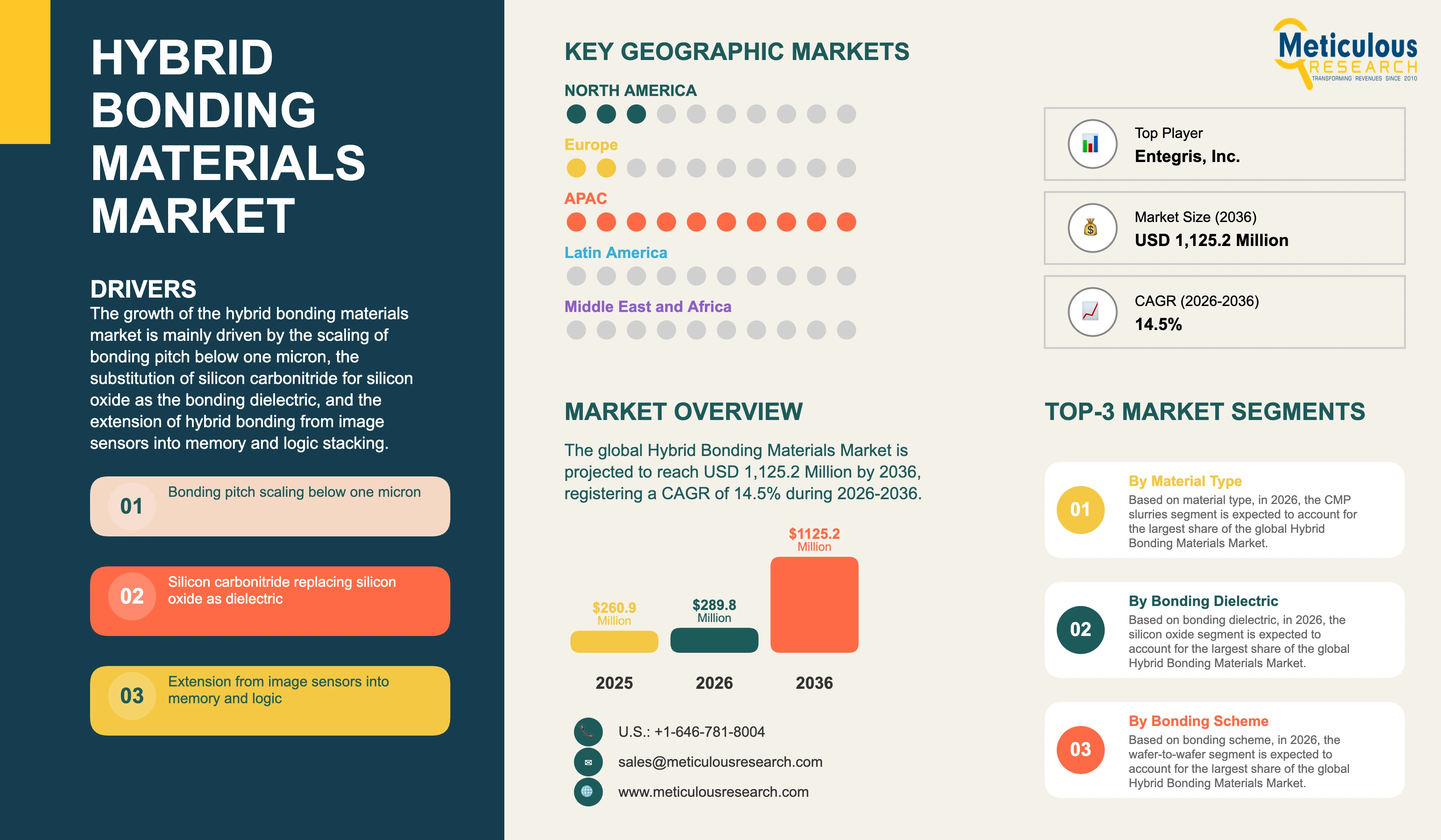
The global hybrid bonding materials market was valued at USD 260.9 million in 2025. This market is expected to reach USD 1,125.2 million by 2036 from an estimated USD 289.8 million in 2026, registering a CAGR of 14.5% during the forecast period (2026-2036).
- Published
- Nov 2026
- Pages
- 268
- Format
- PDF + Excel
- Report ID
- MRCHM - 1042652
- Base year
- 2025
- 2025 · BASELINE
- $260.9M
- 2036
- $1.13B
- CAGR 2026–2036
- 14.5%
2025 baseline · 2026–2036 forecast at 14.5% CAGR · hover a bar for the value
Key highlights
The global hybrid bonding materials market is estimated at USD 289.8 million in 2026 and is projected to reach USD 1,125.2 million by 2036.
Market volume is estimated at 12.60 kilotons in 2026 and is projected to reach 54.62 kilotons by 2036 at a CAGR of 15.8%.
The average selling price is estimated at USD 23.00 per kg in 2026 and is projected to reach USD 20.60 per kg by 2036.
CMP slurries are expected to account for the largest material type share in 2026, while bonding dielectric films and precursors are projected to register the highest CAGR of 17.2%.
Silicon oxide is expected to remain the largest bonding dielectric in 2026, while silicon carbonitride is projected to grow fastest at a CAGR of 21.5%.
Wafer-to-wafer bonding is expected to account for the largest scheme share in 2026, while die-to-wafer bonding is projected to register the highest CAGR of 18.6%.
Interconnect pitch above one micron is expected to hold the largest share in 2026, while pitch below 500 nm is projected to grow fastest at a CAGR of 26.4%.
Image sensors are expected to be the largest end-use application in 2026, while memory is projected to register the highest CAGR of 19.8%.
Asia-Pacific is expected to hold the largest regional share in 2026, while North America is projected to register the highest CAGR of 16.8%.
imec reported 400 nm Cu/SiCN wafer-to-wafer hybrid bonding pitch at IEDM 2023, against a commercial state of the art of about one micron.
Commercial hybrid bonding applications integrate about one million interconnects per square millimetre.
Overlay achieved at 400 nm pitch was below 150 nm, while imec states that overlay control must be below 100 nm for sufficient yield in high-volume manufacturing at that pitch.
Silicon carbonitride has higher bonding energy than silicon oxide, acts as a copper diffusion barrier and gives a more thermally stable interface, reaching high bond strength after a post-bond anneal at 250 degrees Celsius without degrading at higher temperatures.
CMP must leave only a few nanometres of copper pad recess below the dielectric surface for void-free bonding after anneal.
Bonding takes place at room temperature from the wafer centre outward, with the permanent copper and dielectric bonds formed in a subsequent higher-temperature anneal.
Pad layouts have moved from a square grid to a hexagonal grid with circular copper pads, and unequal pad designs showed higher dielectric breakdown strength at small pitches.
FUJIFILM Corporation announced on 29 September 2025 that a major semiconductor device manufacturer had adopted its new CMP slurry for planarizing bonding surfaces in hybrid bonding.
That slurry is an evolution of a front-end copper interconnect slurry and is designed for surfaces where copper and oxide films coexist, with extension planned to redistribution layers and micro-bumps.
FUJIFILM operates CMP slurry plants in Arizona, Hsinchu, Tainan, Cheonan and Kumamoto, and planned operations at a new facility in Zwijndrecht, Belgium from spring 2026.
Report summary
| Particulars | Details |
|---|---|
| Base Year | 2025 |
| Forecast Period | 2026-2036 |
| Market Size in 2025 | USD 260.9 million |
| Market Size in 2026 | USD 289.8 million |
| Market Size by 2036 | USD 1,125.2 million |
| Value CAGR (2026-2036) | 14.5% |
| Format | PDF, Excel & Cloud Portal · 268 pages |
| Volume in 2026 | 12.60 kilotons |
| Volume by 2036 | 54.62 kilotons |
| Volume CAGR (2026-2036) | 15.8% |
| Average Selling Price in 2026 | USD 23.00 per kg |
| Average Selling Price by 2036 | USD 20.60 per kg |
| Measurement Basis | Materials consumed in hybrid bonding flows, covering CMP slurries, bonding dielectric films and precursors, post-CMP cleaning chemistries, copper electroplating chemistries for bond pads, temporary bonding and debonding materials, and surface activation chemistries, excluding bonders, aligners, CMP and deposition equipment, and die attach adhesives, underfills and solder materials used in micro-bump flows |
| Largest Material Type Segment | CMP slurries |
| Fastest-Growing Material Type Segment | Bonding dielectric films and precursors (CAGR 17.2%) |
| Largest Bonding Dielectric | Silicon oxide |
| Fastest-Growing Bonding Dielectric | Silicon carbonitride (CAGR 21.5%) |
| Largest Bonding Scheme | Wafer-to-wafer |
| Fastest-Growing Bonding Scheme | Die-to-wafer (CAGR 18.6%) |
| Largest Interconnect Pitch Segment | Above 1 micron |
| Fastest-Growing Interconnect Pitch Segment | Below 500 nm (CAGR 26.4%) |
| Largest End-Use Application | Image sensors |
| Fastest-Growing End-Use Application | Memory (CAGR 19.8%) |
| Largest Region | Asia-Pacific |
| Fastest-Growing Region | North America (CAGR 16.8%) |
| Segments Covered | Material Type, Bonding Dielectric, Bonding Scheme, Interconnect Pitch, End-Use Application, and Geography |
| Geographies Covered | Asia-Pacific, North America, Europe, Middle East & Africa, and Latin America |
| Companies Profiled | 13 companies, including Entegris, Inc., FUJIFILM Holdings Corporation, Merck KGaA, Resonac Holdings Corporation, Qnity Electronics, Inc., and Tokyo Ohka Kogyo Co., Ltd. |
Report overview
Segments covered: material type, bonding dielectric, bonding scheme, interconnect pitch, end-use application.
In volume terms, this market is estimated at 12.60 kilotons in 2026 and is projected to reach 54.62 kilotons by 2036, registering a CAGR of 15.8% during the same period. The average selling price is estimated at USD 23.00 per kg in 2026 and is projected to decline to USD 20.60 per kg by 2036 as slurry and cleaning chemistry volumes move from qualification quantities to production supply and regional filling capacity is added close to the bonding fabs.
The growth of this market is mainly driven by the scaling of bonding pitch below one micron, which places planarization and dielectric quality rather than tool capability on the critical path, the adoption of silicon carbonitride as the bonding dielectric in place of silicon oxide, the extension of hybrid bonding from image sensors into memory and logic stacking, and the qualification of dedicated advanced packaging slurries by device manufacturers. However, factors such as the overlay control required for yield at sub-micron pitch, and the cost and duration of the qualification cycle that each new material must pass at a device manufacturer, are expected to restrain the growth of this market to some extent.
CMP slurries account for the largest share of this market because the bonding surface has to be planarized to a few nanometres of copper recess across a full 300 mm wafer and the slurry is consumed per wafer pass rather than per die. Bonding dielectric films and precursors grow faster because the move from silicon oxide to silicon carbonitride raises both the material value per wafer and the number of deposition steps in the flow.
Hybrid bonding materials are the consumable materials used to prepare, planarize, clean, activate and bond the copper and dielectric surfaces that form a direct copper-to-copper and dielectric-to-dielectric interconnect between two silicon wafers or between a die and a wafer. Market sizing in this report is on both a value basis in USD and a volume basis in kilotons, with average selling price derived from the two. The measurement basis is the materials consumed in hybrid bonding flows, covering CMP slurries, bonding dielectric films and precursors, post-CMP cleaning chemistries, copper electroplating chemistries for the bond pads, temporary bonding and debonding materials used in carrier flows, and surface activation chemistries. It excludes bonders, aligners, CMP and deposition equipment, and the die attach adhesives, underfills and solder materials used in micro-bump flows.
The process begins from fully processed 300 mm wafers with completed front-end and back-end of line, according to imec, which reported 400 nm Cu/SiCN wafer-to-wafer hybrid bonding pitch at IEDM 2023 and published the result on 19 February 2024. Bonding occurs at room temperature and starts at the wafer centre, with a bonding wave closing the gap out to the edge, and the permanent copper-to-copper and dielectric-to-dielectric bonds form during a subsequent higher-temperature anneal. No adhesive is present in the joint, which is what distinguishes this route from every other bonding method and is why the materials market sits in surface preparation rather than in adhesives.
Planarization sets the limit on what can be bonded. CMP must produce an extremely flat dielectric surface with only a few nanometres of recess for the copper pads, since the copper has to sit slightly below the dielectric before bonding for the joint to close void-free during anneal. Advanced CMP combined with dummy pads was required to control copper pad height and surface topology across the full wafer at 400 nm pitch. The slurry is therefore specified against a nanometre-scale topography target across 300 mm rather than against a removal rate, and it has to planarize a surface where copper and oxide films coexist.
The bonding dielectric is changing. Current process flows predominantly use silicon oxide, while silicon carbonitride is the proposed dielectric for small pitches because it has higher bonding energy than silicon oxide, acts as a copper diffusion barrier and gives a more thermally stable interface. Nanoindentation measurements showed silicon carbonitride to silicon carbonitride bond strength significantly exceeding silicon oxide to silicon oxide, and the material reaches high bond strength after a post-bond anneal at 250 degrees Celsius without degrading at higher temperatures. The substitution raises the value of the dielectric per wafer and changes the precursor supply chain behind it.
Pitch scaling is the demand driver and it is documented against specific numbers. Commercial applications integrate about one million interconnects per square millimetre at a copper interconnect pitch of about one micron, memory-on-logic stacking requires pitches far below one micron, and the 3D interconnect landscape spans from millimetres down to less than 100 nm. imec reported 400 nm Cu/SiCN pitch at IEDM 2023 using a hexagonal grid with circular copper pads in place of the traditional square grid, with unequal pad designs in which the top wafer carries smaller critical copper pad dimensions showing higher dielectric breakdown strength at small pitches.
Yield at those pitches is governed by overlay. Overlay achieved at 400 nm pitch was below 150 nm, while imec states that overlay control must be below 100 nm for sufficient yield in high-volume manufacturing. That requirement bears on the materials as well as the tool, because dielectric film stress and thickness uniformity across the wafer contribute to the distortion that overlay has to correct for, and particles left on a bonding surface create voids that no alignment can recover. Cleaning chemistry and filtration consequently sit alongside the slurry rather than behind it.
Material supply is moving from qualification to production. FUJIFILM Corporation announced on 29 September 2025 that a major semiconductor device manufacturer had adopted its new CMP slurry for planarizing bonding surfaces in hybrid bonding, describing the product as an evolution of its front-end copper interconnect slurry and designed for surfaces where copper and oxide films coexist, with extension planned to redistribution layers and micro-bumps. The company operates CMP slurry plants in Arizona, Hsinchu, Tainan, Cheonan and Kumamoto, and planned operations at a new facility in Zwijndrecht, Belgium from spring 2026. A front-end slurry reformulated for a packaging step indicates where the technical capability for this market already sits.
The materials are front-end grade sold into a packaging step, and that is what sets the economics. Purity, particle count and lot-to-lot consistency are specified at front-end interconnect levels because the bonding surface becomes a buried interconnect interface rather than an external package feature, while the volumes are those of a packaging line rather than of a full wafer fab. The result is a small market by mass with high value per kilogram, supplied by companies whose qualification position in front-end CMP and cleaning gives them the only practical route in.
Silicon oxide is expected to hold the largest share in 2026, as it predominates in current process flows.
Silicon carbonitride is projected to register the highest CAGR of 21.5% during the forecast period.
Wafer-to-wafer bonding is expected to account for the largest share in 2026.
Die-to-wafer bonding is projected to register the highest CAGR of 18.6% during the forecast period.
Image sensors are expected to hold the largest share in 2026, as the first application to reach volume hybrid bonding production.
Memory is projected to register the highest CAGR of 19.8% during the forecast period.
Asia-Pacific is expected to account for the largest share in 2026, supported by the concentration of image sensor, memory and advanced logic manufacturing in Taiwan, South Korea, Japan and China. Taiwan is projected to grow at 13.6% and South Korea at 15.2%.
North America is projected to register the highest CAGR of 16.8% during the forecast period, with the United States at 17.0%.
Europe is projected to grow at a CAGR of 14.2%, with Germany at 13.8%. The regional position rests on research and on materials and equipment supply rather than on volume bonding, with the 400 nm Cu/SiCN pitch work originating at imec and FUJIFILM Corporation planning operations at a new slurry facility in Zwijndrecht, Belgium from spring 2026.
The Middle East & Africa is projected to grow at a CAGR of 15.4% and Latin America at a CAGR of 11.0%, both from very small bases where assembly and test rather than bonding capacity accounts for the activity.
Entegris, Inc., FUJIFILM Holdings Corporation, Merck KGaA, Resonac Holdings Corporation and Qnity Electronics, Inc. together accounted for an estimated 54.8% of this market in 2026. The 13 companies profiled in this report together accounted for an estimated 81.5%.
Report infographic
Market dynamics
15 factors across 5 forcesBonding Pitch Scaling Below One Micron
Commercial hybrid bonding integrates about one million interconnects per square millimetre at a copper pitch of about one micron, memory-on-logic stacking requires pitches far below one micron, and imec reported 400 nm Cu/SiCN wafer-to-wafer pitch at IEDM 2023. Each step down in pitch tightens the copper recess and dielectric flatness that CMP has to deliver across a 300 mm wafer and reduces the particle size that cleaning has to remove, because a defect comparable to the pad dimension now destroys an interconnect rather than a fraction of one. Pad layouts have moved to a hexagonal grid with circular copper pads and to unequal designs in which the top wafer carries smaller critical dimensions, which changes the pattern density the slurry sees. Material specification therefore tightens with every pitch node, and the qualification position earned at one pitch does not carry forward to the next without new work. The particle specification tightens on the same schedule, since a defect comparable to the pad dimension now destroys an interconnect outright rather than degrading one, which pulls filtration and cleaning into the same qualification as the slurry.
Substitution of Silicon Carbonitride for Silicon Oxide as the Bonding Dielectric
Current process flows predominantly use silicon oxide, while silicon carbonitride is the proposed dielectric for small pitches, with higher bonding energy than silicon oxide, a copper diffusion barrier function and a more thermally stable interface. Nanoindentation measurements showed silicon carbonitride bond strength significantly exceeding that of silicon oxide, and the film reaches high bond strength after a post-bond anneal at 250 degrees Celsius without degrading at higher temperatures. The substitution replaces a commodity oxide precursor with a carbon and nitrogen containing precursor at higher cost per wafer and brings the deposition chemistry supplier into the bonding decision. It also raises the share of this market held by dielectric films and precursors relative to the planarization and cleaning materials around them.
Extension from Image Sensors into Memory and Logic Stacking
Hybrid bonding entered production in image sensors, where the stack is two wafers of known good area and the pitch requirement is modest, and the technology is now being applied to memory stacking and to logic partitioning where the interconnect count per square millimetre is far higher. The 3D interconnect landscape spans from millimetres down to less than 100 nm, and the move toward the lower end of that range is what memory-on-logic stacking requires. Each new application brings a different pattern density, a different metal fraction on the bonding surface and a different thermal budget, none of which a single slurry or cleaning chemistry covers. Material suppliers consequently sell a portfolio qualified per application rather than one product, which multiplies the revenue per material platform. The breadth also favours suppliers already running several front-end material lines, because a portfolio qualified per application cannot be assembled from a single chemistry.
Qualification of Dedicated Advanced Packaging Materials by Device Manufacturers
FUJIFILM Corporation announced on 29 September 2025 that a major semiconductor device manufacturer had adopted its new CMP slurry for planarizing bonding surfaces in hybrid bonding, a product evolved from its front-end copper interconnect slurry and designed for surfaces where copper and oxide films coexist. The company planned operations at a new facility in Zwijndrecht, Belgium from spring 2026 alongside existing plants in Arizona, Hsinchu, Tainan, Cheonan and Kumamoto, and plans to extend the product to redistribution layers and micro-bumps. An adoption of this kind converts a development material into a production consumable with a committed volume behind it. It also establishes the supply pattern for the market, in which front-end material platforms are reformulated for the bonding step rather than developed from nothing.
Table of contents
13 chapters · 142 sections · 268 pages · click to expandSegmental analysis
| Segment | Largest share (2026) | Fastest growth (2026–2036) |
|---|---|---|
| By Material Type | CMP slurries | — |
| Other segments | — | Bonding dielectric films and precursors |
By Material Type
- CMP slurries are expected to account for the largest share in 2026, supported by the nanometre-scale planarization requirement and by consumption per wafer pass.
- Pitch above one micron is expected to hold the largest share in 2026, matching the commercial state of the art of about one micron with roughly one million interconnects per square millimetre.
Other segments
- Bonding dielectric films and precursors are projected to register the highest CAGR of 17.2% during the forecast period.
- Pitch below 500 nm is projected to register the highest CAGR of 26.4% during the forecast period.
Geographic analysis
Asia-Pacific
Largest shareIn 2026, Asia-Pacific is expected to account for the largest share of the global hybrid bonding materials market. The large share of this region is mainly due to the concentration of image sensor, memory and advanced logic manufacturing in Taiwan, South Korea, Japan and China where hybrid bonding capacity is installed, the presence of the CMP slurry, cleaning chemistry and precursor suppliers that serve those fabs, and the slurry filling plants FUJIFILM Corporation operates in Hsinchu, Tainan, Cheonan and Kumamoto close to that demand. Taiwan is projected to register a CAGR of 13.6% and South Korea a CAGR of 15.2% during the forecast period.
North America
Fastest growthHowever, North America is projected to register the highest CAGR of 16.8% during the forecast period. The rapid growth of this region is attributed to the advanced packaging capacity being added alongside new front-end fabs in the United States, the logic partitioning applications that drive the smallest pitch requirements and the materials that go with them, and the existing slurry filling capacity in Arizona that allows local supply as those lines qualify. The United States is projected to register a CAGR of 17.0% during the forecast period.
Europe
Europe holds a smaller share concentrated in research and in equipment and materials supply rather than in volume bonding, and is projected to grow at 14.2%, with Germany at 13.8%. The research position is substantial, since the 400 nm Cu/SiCN pitch and the overlay and pad design work behind it came from imec, and FUJIFILM Corporation planned operations at a new slurry facility in Zwijndrecht, Belgium from spring 2026.
Middle East & Africa
The Middle East & Africa is projected to grow at 15.4% and Latin America at 11.0%, both from very small bases where assembly and test rather than bonding capacity accounts for the activity. Material supply follows bonding capacity more closely in this market than in most, because slurries and cleaning chemistries have limited shelf life and are sensitive to transport conditions, and because qualification is granted per site. A supplier qualified at a fab in one region cannot serve a second site in another region from the same plant without requalification against the shipped material. That is the reason filling capacity is being placed in Arizona, Taiwan, South Korea, Japan and now Belgium rather than consolidated, and it gives regional presence a weight in supplier selection that formulation alone does not carry. Proximity also shortens the feedback loop during qualification, when a formulation adjustment has to reach the line within the window of a scheduled wafer lot rather than in the next quarter.
Competitive landscape
The global hybrid bonding materials market is characterised by the presence of electronic materials specialists, diversified chemical and imaging companies with front-end semiconductor materials positions, industrial gas companies supplying deposition precursors, and specialists in temporary bonding materials for carrier flows. Competition is contested on qualification position at the device manufacturer rather than on formulation, since the bonding interface is buried and cannot be reworked and a material change has to be proven against overlay and topography on committed wafers. Entegris, Inc., FUJIFILM Holdings Corporation, Merck KGaA, Resonac Holdings Corporation and Qnity Electronics, Inc. together accounted for an estimated 54.8% of this market in 2026, while the companies profiled in this report together accounted for an estimated 81.5%.
FUJIFILM Corporation announced on 29 September 2025 that a major semiconductor device manufacturer had adopted its new CMP slurry for planarizing bonding surfaces in hybrid bonding, an evolution of its front-end copper interconnect slurry designed for surfaces where copper and oxide films coexist, with extension planned to redistribution layers and micro-bumps and operations planned at a new facility in Zwijndrecht, Belgium from spring 2026. DuPont completed the separation of its electronics business as Qnity Electronics, Inc. on 1 November 2025, which placed the CMP pad and slurry portfolio in an independent public company focused on electronic materials. Qualification wins at device manufacturers and regional filling capacity accounted for most competitive activity through 2026.
The suppliers able to compete here are those already qualified in front-end interconnect materials, because the bonding surface is specified at front-end purity and particle levels and the material platforms are reformulations of front-end slurries, cleaners and precursors rather than new products. Industrial gas companies hold the precursor position behind the silicon carbonitride substitution, while temporary bonding specialists serve the die-to-wafer carrier flows. Some of the key players operating in the hybrid bonding materials market are Entegris, Inc. (U.S.), FUJIFILM Holdings Corporation (Japan), Merck KGaA (Germany), Resonac Holdings Corporation (Japan), Qnity Electronics, Inc. (U.S.), Tokyo Ohka Kogyo Co., Ltd. (Japan), JSR Corporation (Japan), Shin-Etsu Chemical Co., Ltd. (Japan), Air Liquide S.A. (France), Linde plc (U.K.), Nitto Denko Corporation (Japan), Brewer Science, Inc. (U.S.), and Soulbrain Co., Ltd. (South Korea), among others.
- —
FUJIFILM Corporation announced on 29 September 2025 that a major semiconductor device manufacturer had adopted its new CMP slurry for planarizing bonding surfaces in hybrid bonding, with operations planned at a new facility in Zwijndrecht, Belgium from spring 2026. DuPont completed the separation of its electronics business as Qnity Electronics, Inc. on 1 November 2025. imec published its 400 nm Cu/SiCN wafer-to-wafer hybrid bonding pitch results on 19 February 2024, following their presentation at IEDM 2023.
- Entegris, Inc.
- FUJIFILM Holdings Corporation
- Merck KGaA
- Resonac Holdings Corporation
- Qnity Electronics, Inc.
- Tokyo Ohka Kogyo Co., Ltd
Expert perspectives
Volume grows at 15.8% against 14.5% in value over the forecast period, and the average selling price falls from USD 23.00 per kg in 2026 to USD 20.60 per kg by 2036 as slurry and cleaning chemistry volumes move from qualification quantities to production supply and filling capacity is added close to the bonding fabs. The decline is a volume effect rather than a competitive one, since qualification position rather than price determines who supplies a bonded wafer.
What is being sold is topography control, not chemistry. CMP has to leave only a few nanometres of copper pad recess across a fully processed 300 mm wafer, and advanced CMP combined with dummy pads was required to achieve that at 400 nm pitch. A slurry is therefore specified against a nanometre-scale target on a surface carrying copper and oxide at varying pattern density, which is why a front-end interconnect slurry rather than a packaging material was the platform FUJIFILM reformulated for the step.
The dielectric transition is the largest value change in this market. Silicon carbonitride replaces silicon oxide at small pitches on the strength of higher bonding energy, a copper diffusion barrier function and a stable interface after a 250 degrees Celsius post-bond anneal, and imec used Cu/SiCN for the 400 nm pitch work reported at IEDM 2023. A carbon and nitrogen containing precursor costs more per wafer than a commodity oxide and brings the gas supplier into the bonding decision, which is why dielectric films and precursors grow fastest among the material types.
Overlay rather than material capability sets the pace. Overlay achieved at 400 nm pitch was below 150 nm while imec states that below 100 nm is needed for sufficient yield in high-volume manufacturing, and film stress and thickness uniformity feed directly into the wafer distortion that overlay has to correct. The materials market scales with bonded wafers rather than with demonstrated pitch, so the sub-micron material demand arrives when that yield gap closes and not before.
The interface cannot be reworked, and that governs supplier behaviour more than any technical specification. Bonds form permanently during the post-bond anneal between two fully processed wafers, so a defect introduced by a material destroys the value of both and cannot be inspected afterwards. Device manufacturers consequently hold incumbent materials for longer than performance alone would justify, which is the mechanism concentrating an estimated 54.8% of this market with five suppliers.
Die-to-wafer bonding is where material content per bonded area is highest. Placing known good and dissimilar sized die requires carriers, temporary bonding, debonding and additional cleaning that wafer-to-wafer bonding avoids entirely, while each die still has to arrive with full-wafer planarity and cleanliness. The scheme grows faster than wafer-to-wafer bonding for yield reasons, and the material intensity means its share of value rises faster than its share of bonded area.
Customer perspectives
Planarization uniformity across a patterned 300 mm wafer rather than removal performance is the selection criterion, and the pattern density of the product is part of the qualification.
The dielectric transition is being brought forward for downstream process reasons, and precursor qualification is being written against wafer-level distortion rather than film properties alone.
The absence of rework and inspection at a buried interface makes material changes rare and gives regional filling capacity a weight in supplier selection that formulation alone does not carry.
“Our constraint is not the bonder, it is what the surface looks like before it reaches the bonder. We need copper a few nanometres below the dielectric and we need it uniform across the whole wafer, and that is a slurry and a pad design problem together. A material that polishes beautifully on a blanket wafer and then fails on our pattern density is of no use to us.”
“We are moving to the nitride dielectric before our pitch strictly requires it, because the diffusion barrier and the thermal stability make everything downstream easier. That changes our precursor supply and it changes film stress, which goes straight into our overlay budget. We qualify the precursor against wafer distortion, not just against film composition.”
“Once those two wafers are bonded and annealed, there is no going back and no inspecting the interface. One particle is a void and the void is permanent. That is why we are slow to change a cleaning chemistry and why we want the material filled in the same region we run in, not shipped halfway around the world.”
Frequently asked questions
This market was valued at USD 235.2 million in 2024 and USD 260.9 million in 2025, and is estimated at USD 289.8 million in 2026. In volume terms it is estimated at 12.60 kilotons in 2026.
Cite this report
Meticulous Research. (2026). Hybrid Bonding Materials Market - Global Opportunity Analysis and Industry Forecast (2026-2036) (Report No. MRCHM - 1042652). Meticulous Market Research Pvt. Ltd. https://www.meticulousresearch.com/product/hybrid-bonding-materials-market-7335