Extreme Ultraviolet (EUV) Lithography Materials Market (2026-2036)
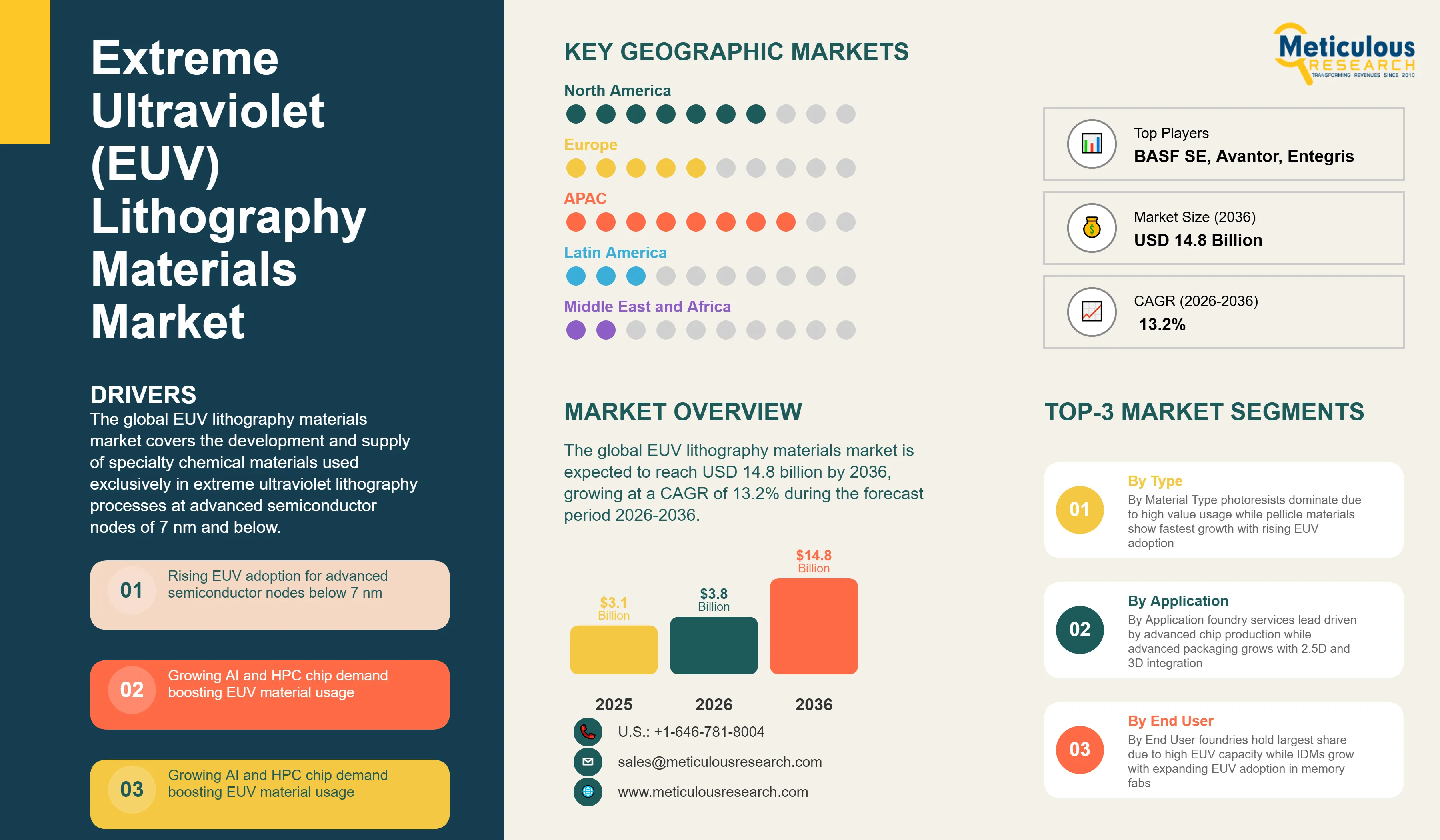
The global EUV lithography materials market was valued at USD 3.1 billion in 2025. This market is expected to reach USD 14.8 billion by 2036 from an estimated USD 3.8 billion in 2026, growing at a CAGR of 13.2% during the forecast period 2026-2036.
- Published
- Apr 2026
- Pages
- 288
- Format
- PDF + Excel
- Report ID
- MR-1889
- Base year
- 2025
- 2025 · BASELINE
- $3.10B
- 2036
- $14.80B
- CAGR 2026–2036
- 13.2%
2025 baseline · 2026–2036 forecast at 13.2% CAGR · hover a bar for the value
Key highlights
The global EUV lithography materials market is projected to reach USD 14.8 billion by 2036.
The market is expected to grow at a CAGR of 13.2% during the forecast period 2026-2036.
The market was valued at USD 3.1 billion in 2025 and is estimated to reach USD 3.8 billion in 2026.
Asia-Pacific is expected to dominate the global EUV lithography materials market with the largest market share in 2026.
By material type, the photoresists segment is expected to hold the largest share in 2026.
By process step, the coating segment is expected to hold the largest share in 2026.
By technology node, the 3 nm segment is expected to hold the largest share in 2026.
By application, the foundry services segment is expected to hold the largest share in 2026.
By end user, the foundries segment is expected to hold the largest share in 2026.
By resist type, the organic (CAR-based) resists segment is expected to hold the largest share in 2026, while metal-oxide resists is the fastest growing segment.
Report summary
| Particulars | Details |
|---|---|
| Market Size by 2036 | USD 14.8 Billion |
| Market Size in 2026 | USD 3.8 Billion |
| Market Size in 2025 | USD 3.1 Billion |
| Revenue Growth Rate (2026-2036) | CAGR of 13.2% |
| Format | PDF, Excel & Cloud Portal · 288 pages |
| Dominating Material Type | Photoresists |
| Fastest Growing Material Type | Pellicle Materials |
| Dominating Process Step | Coating |
| Fastest Growing Process Step | Post-Processing |
| Dominating Technology Node | 3 nm |
| Fastest Growing Technology Node | 2 nm and Below |
| Dominating Application | Foundry Services |
| Fastest Growing Application | Advanced Packaging |
| Dominating End User | Foundries |
| Fastest Growing End User | IDMs |
| Dominating Resist Type | Organic (CAR-Based) Resists |
| Fastest Growing Resist Type | Metal-Oxide Resists |
| Dominating Geography | Asia-Pacific |
| Fastest Growing Geography | North America |
| Base Year | 2025 |
| Forecast Period | 2026 to 2036 |
Report overview
Segments covered: material type, process step, technology node, application.
The global EUV lithography materials market covers the development and supply of specialty chemical materials used exclusively in extreme ultraviolet lithography processes at advanced semiconductor nodes of 7 nm and below. The market encompasses photoresist formulations including chemically amplified and metal-oxide resist platforms, anti-reflective and top-coat materials, developers, ancillary processing chemicals, EUV mask blanks and absorber materials, pellicle films, and cleaning chemicals designed for compatibility with 13.5 nm wavelength EUV exposure systems. These materials collectively enable high-resolution sub-20 nm feature patterning across logic, memory, and foundry manufacturing applications at TSMC, Samsung Foundry, Intel Foundry, SK Hynix, and Micron.
The growth of the EUV lithography materials market is driven by the accelerating ramp of EUV scanner utilization at leading semiconductor manufacturers and the progressive increase in EUV layer counts per wafer at each successive technology node, from approximately 5 to 8 EUV layers at 7 nm to over 20 EUV layers at 2 nm node generations. The transition to high-NA EUV lithography, with ASML's EXE:5000 system beginning production qualification at TSMC and Intel, is expected to require entirely new photoresist and ancillary chemical formulations optimized for the higher numerical aperture exposure conditions that impose more stringent sensitivity, resolution, and stochastic performance requirements than current-generation EUV systems.
The market faces structural constraints including the very small global supplier base for EUV-qualified photoresist, with JSR Corporation, Tokyo Ohka Kogyo, Shin-Etsu Chemical, and Merck KGaA collectively accounting for the substantial majority of qualified EUV resist supply. Multi-year qualification cycles at each semiconductor customer, combined with the extreme sensitivity of EUV process yield to photoresist performance variability, create significant barriers to new supplier entry and limit the competitive dynamics of the photoresist market. The high development cost of new EUV resist platforms, which require extensive synthesis, formulation, and process integration investment before any commercial revenue is generated, constrains the pace of new material development.
Despite these constraints, the market outlook remains strongly positive. The structural expansion of EUV lithography into memory manufacturing, where SK Hynix and Micron are introducing EUV into DRAM fabrication for the first time, is expanding the EUV materials addressable market beyond its initial logic and foundry concentration. The substantial venture and corporate investment flowing into metal-oxide resist development platforms, which offer potential sensitivity and resolution advantages over chemically amplified resists for high-NA EUV applications, is creating competitive innovation pressure that is accelerating overall EUV materials technology development across the supplier ecosystem.
Report infographic
Market dynamics
7 factors across 3 forcesIncreasing Adoption of EUV for Advanced Nodes (7 nm and Below)
The high-volume manufacturing ramp of EUV lithography at TSMC, Samsung Foundry, and Intel Foundry across successive technology generations from 7 nm through 3 nm and toward 2 nm is the primary structural driver of EUV materials demand. Each node transition increases the number of EUV layers per wafer, directly multiplying photoresist and ancillary chemical consumption per wafer pass. TSMC's N2 process requires over 20 EUV exposures per wafer, compared to approximately 5 at its N7 node, creating a compound materials consumption growth that substantially exceeds aggregate wafer volume growth. The mandatory adoption of EUV for sub-5 nm patterning, where no viable alternative multi-patterning approach exists at acceptable cost and yield, makes EUV materials demand structurally inelastic with respect to node advancement.
Growth of AI, HPC, and Advanced Semiconductor Devices
The exceptional demand growth for AI training and inference accelerator chips, high-performance computing processors, and high-bandwidth memory driven by the rapid commercialization of generative AI applications is sustaining above-trend production ramp at the EUV-equipped leading-edge fabs manufacturing these devices. Nvidia's H100 and B100 GPU series, AMD's MI300 accelerators, and custom AI silicon from Google, Microsoft, and Amazon are all manufactured at TSMC 5 nm and 3 nm nodes with high EUV layer counts, creating sustained and growing demand for EUV photoresist and ancillary materials per production wafer. High-bandwidth memory for AI accelerators, which SK Hynix and Micron are now manufacturing with EUV patterning steps, is extending EUV material demand into the memory segment for the first time at commercial volume.
Table of contents
14 chapters · 170 sections · 288 pages · click to expandSegmental analysis
| Segment | Largest share (2026) | Fastest growth (2026–2036) |
|---|---|---|
| By Material Type | Photoresists | Pellicle materials |
| By Application | Foundry Services | Advanced packaging |
| By End User | Foundries | IDMs |
| By Resist Type | Organic (CAR-Based) Resists | Metal-oxide resists |
By Material Type
- Photoresists to Dominate
- The photoresists segment is expected to account for the largest share of the global EUV lithography materials market.
- Photoresists command the highest unit value of any EUV material category, with EUV photoresist formulations priced at three to five times the equivalent DUV photoresist cost per unit volume, and their consumption scales directly with EUV layer count per wafer.
- The dominant EUV photoresist suppliers including JSR, Tokyo Ohka Kogyo, Shin-Etsu Chemical, and Merck KGaA collectively serve all major EUV-equipped semiconductor manufacturers globally with qualified resist platforms covering both chemically amplified and emerging metal-oxide resist types.
- However, the pellicle materials segment is projected to register the highest CAGR during the forecast period.
- Pellicle adoption is expanding rapidly across EUV-equipped fabs as mask cost economics make contamination protection highly valuable, and the commercialization of high-NA EUV lithography will impose even more stringent pellicle performance requirements that are driving sustained investment in new pellicle material platforms by ASML, Mitsui Chemicals, and Imec.
- Coating to Hold the Largest Share
- The coating segment is expected to account for the largest share of the market.
- The coating step encompasses photoresist coat, anti-reflective coating deposition, and top-coat application, each requiring specialty chemical formulations that collectively represent the highest-value material consumption in the EUV process sequence.
- Photoresist coat alone accounts for the largest single chemical cost per EUV wafer pass.
- However, the post-processing segment is projected to register the highest CAGR, driven by the increasing chemical complexity of resist strip, clean, and defect removal process steps required to achieve the low defect densities demanded by advanced node yield targets and by the growing adoption of selective etch and clean chemistries designed for compatibility with gate-all-around transistor process flows.
- 3 nm to Hold the Largest Share
- The 3 nm segment is expected to account for the largest share of the market, reflecting the concentration of leading-edge high-volume EUV production at TSMC's N3E node and Samsung's SF3 node, which together represent the highest current EUV wafer volume with the highest EUV layer count of any commercially ramped process generation.
- However, the 2 nm and below segment is projected to register the highest CAGR during the forecast period, as TSMC's N2 production ramp and Samsung's SF2 gate-all-around node volume growth drive the highest per-wafer EUV materials consumption of any process generation, and as high-NA EUV introduction at sub-2 nm nodes creates an entirely new materials development and qualification cycle.
By Application
- Foundry Services to Hold the Largest Share
- The foundry services segment is expected to account for the largest share, driven by TSMC's dominant position as the world's most advanced and highest-volume EUV manufacturing facility serving the fabless semiconductor ecosystem for AI, mobile, and high-performance computing chip production.
- TSMC's N3 and N2 production nodes represent the highest concentration of EUV scanner utilization and materials consumption of any individual manufacturing entity globally.
- However, the advanced packaging segment is projected to register the highest CAGR during the forecast period.
- The adoption of EUV-resolution lithography for redistribution layer patterning in 2.5D and 3D integrated circuit packages is extending EUV materials consumption into the back-end packaging domain, creating new addressable volume for EUV photoresist and ancillary chemical suppliers beyond traditional front-end wafer fabrication.
By End User
- Foundries to Hold the Largest Share
- The foundries segment is expected to account for the largest share, with TSMC, Samsung Foundry, and GlobalFoundries collectively operating the majority of installed EUV scanner capacity and consuming the largest share of EUV materials by value.
- The foundry business model's concentration of the most advanced process node manufacturing at a small number of facilities creates the highest EUV material consumption intensity per organization in the semiconductor industry.
- However, the IDMs segment is projected to register the highest CAGR, driven by Intel Foundry's accelerating EUV ramp across its 18A and 14A advanced process nodes at Ohio and Ireland manufacturing facilities, and by SK Hynix and Micron's introduction of EUV patterning into DRAM manufacturing that is expanding IDM EUV material consumption into the memory segment for the first time at commercial production scale.
By Resist Type
- Organic (CAR-Based) Resists to Hold the Largest Share
- The organic CAR-based resists segment is expected to account for the largest share, reflecting the established commercial qualification status of chemically amplified resist platforms from JSR, Tokyo Ohka Kogyo, and Shin-Etsu Chemical at all current EUV production nodes from 7 nm through 3 nm.
- CAR-based resists benefit from decades of formulation refinement, broad fab process integration knowledge, and existing supply chain infrastructure that metal-oxide platforms are still building.
- However, the metal-oxide resists segment is projected to register the highest CAGR during the forecast period.
- The ongoing production qualification programs for tin-oxide and hafnium-oxide resist platforms at TSMC N2 and Samsung SF2 are advancing metal-oxide resists toward their first high-volume manufacturing design-in, and the transition to high-NA EUV will accelerate metal-oxide adoption given the inherent sensitivity and resolution advantages of inorganic resist systems at the extreme imaging conditions of high-NA exposure.
- This segment is critical for differentiation and premium pricing in the EUV materials market.
Geographic analysis
Asia-Pacific
Largest shareIn 2026, Asia-Pacific is expected to account for the largest share of the global EUV lithography materials market. The region's dominant position reflects the concentration of all commercial EUV lithography manufacturing in Taiwan, South Korea, and Japan. TSMC's Hsinchu and Tainan fab complex in Taiwan operates the world's largest fleet of ASML EUV scanners and represents the single largest EUV materials consumption entity globally. Samsung Foundry and SK Hynix in South Korea collectively operate the second largest EUV scanner installed base, serving both foundry customers and Samsung's internal logic and memory chip requirements. Japan's strategic role as the dominant supplier of EUV photoresists, mask materials, and specialty chemicals to global semiconductor manufacturers positions Japanese chemical producers including JSR, Tokyo Ohka Kogyo, Shin-Etsu Chemical, Fujifilm, and Sumitomo Chemical as the primary beneficiaries of EUV materials market growth, even as their customers are located across Asia, North America, and Europe.
North America
Fastest growthHowever, North America is expected to grow at the fastest CAGR during the forecast period. The unprecedented U.S. semiconductor fab investment catalyzed by the CHIPS and Science Act is establishing a major new EUV manufacturing cluster across TSMC Fab 21 in Arizona, Intel's Ohio campus, and Samsung's Taylor Texas facility, all of which will operate advanced EUV-equipped process nodes requiring substantial local or regionally sourced specialty material supply. As these facilities ramp from equipment installation toward full production through the 2026-2030 period, North America's share of global EUV materials consumption will grow significantly from its current modest level. U.S.-based EUV material suppliers including Entegris, DuPont, Brewer Science, and Avantor are positioned to expand their roles in the emerging U.S. EUV supply ecosystem alongside Japanese and European suppliers establishing U.S. production facilities.
Europe
Europe holds a strategically significant position in the EUV materials ecosystem anchored by ASML in Eindhoven, Netherlands, which is the world's sole manufacturer of EUV lithography systems and whose R&D activities drive the specification requirements for EUV material development globally. The Netherlands, Belgium, and Germany host multiple EUV-related research programs including IMEC in Leuven, which serves as a global collaborative center for EUV process and materials development, attracting chemical supplier R&D investment and enabling early-stage process integration evaluations for next-generation EUV material platforms before production qualification at leading semiconductor manufacturers.
Competitive landscape
- JSR Corporation · Japan
- Tokyo Ohka Kogyo Co. Ltd. · Japan
- Shin-Etsu Chemical Co. Ltd. · Japan
- Fujifilm Holdings Corporation · Japan
- Merck KGaA · Germany
- DuPont de Nemours Inc. (U.S.)
- Sumitomo Chemical Co. Ltd. · Japan
- Dongjin Semichem Co. Ltd. · South Korea
- LG Chem Ltd. · South Korea
- Samsung SDI Co. Ltd. · South Korea
- BASF SE · Germany
- Avantor Inc. (U.S.)
- Brewer Science Inc. (U.S.)
- Allresist GmbH · Germany
- Entegris Inc. (U.S.)
Frequently asked questions
The global EUV lithography materials market is expected to reach USD 14.8 billion by 2036 from an estimated USD 3.8 billion in 2026, at a CAGR of 13.2% during the forecast period 2026-2036.
Cite this report
Meticulous Research. (2026). Extreme Ultraviolet (EUV) Lithography Materials Market - Global Opportunity Analysis and Industry Forecast (2026-2036) (Report No. MR-1889). Meticulous Market Research Pvt. Ltd. https://www.meticulousresearch.com/product/extreme-ultraviolet-lithography-materials-market-6572