CMP Slurries and Pads Market (2026-2036)
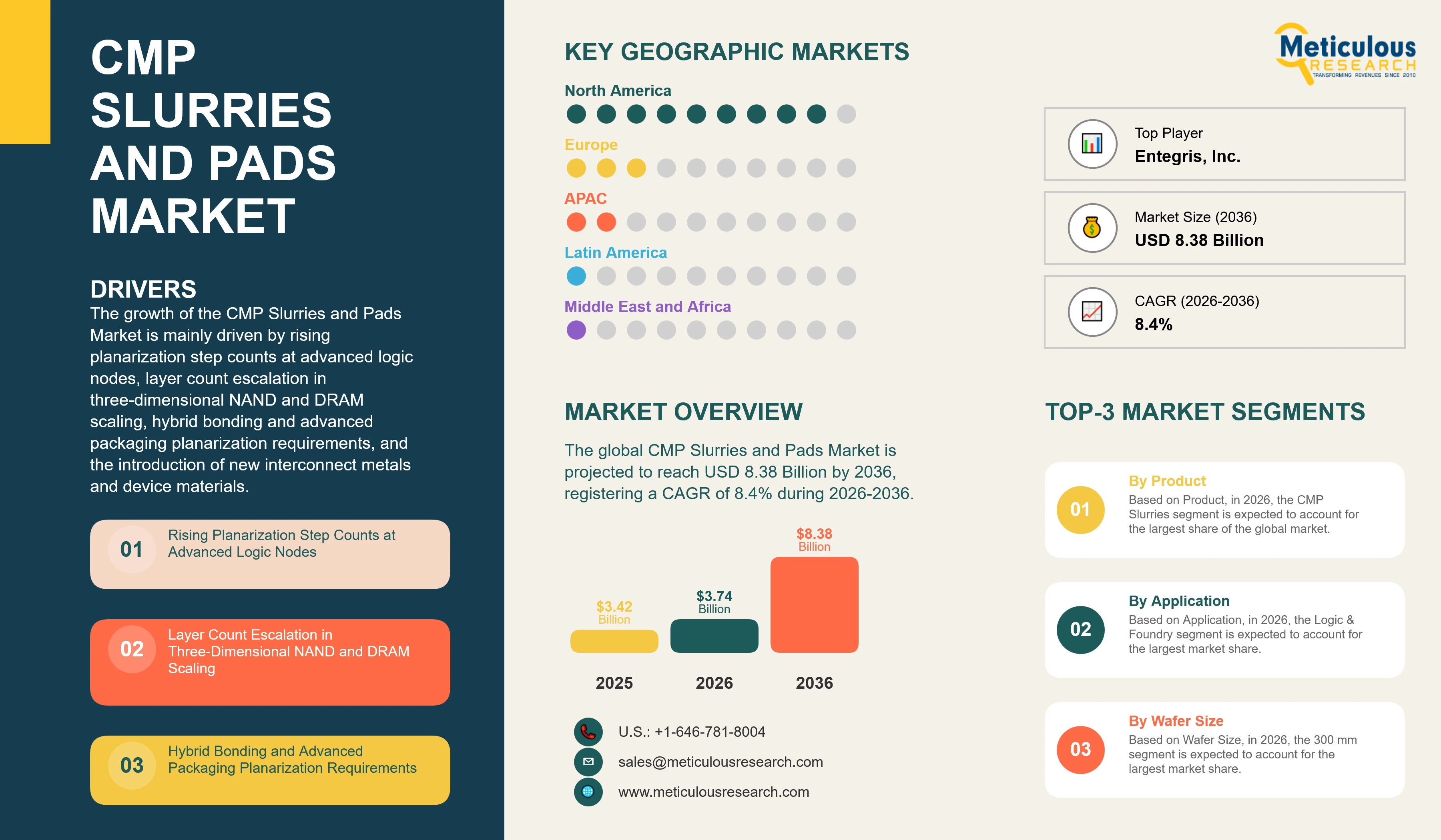
The global CMP Slurries and Pads Market was valued at USD 3.42 billion in 2025. This market is expected to reach USD 8.38 billion by 2036 from an estimated USD 3.74 billion in 2026, registering a CAGR of 8.4% during the forecast period (2026-2036).
- Published
- Oct 2026
- Pages
- 290
- Format
- PDF + Excel
- Report ID
- MRCHM - 1042378
- Base year
- 2025
- 2025 · BASELINE
- $3.42B
- 2036
- $8.38B
- CAGR 2026–2036
- 8.4%
2025 baseline · 2026–2036 forecast at 8.4% CAGR · hover a bar for the value
Key highlights
The global CMP Slurries and Pads Market is projected to reach USD 8.38 billion by 2036, driven by rising planarization step counts at advanced nodes, three-dimensional NAND tier escalation, hybrid bonding in advanced packaging, and new interconnect metal chemistries.
Consumable demand is growing more slowly than the wider materials cycle. In the second quarter of 2026, ended 27 June 2026, Entegris, Inc., whose product range includes chemical mechanical planarization slurries and pads, reported revenue of USD 883.2 million, up approximately 11.5% from USD 792.4 million a year earlier, with Materials Solutions segment revenue of USD 371.3 million, up approximately 4.6%, and Advanced Purity Solutions revenue of USD 514.6 million, up approximately 17.0%.
Supplier margins are nonetheless expanding. Entegris reported second-quarter 2026 gross margin of 47.6% against 44.4% a year earlier and adjusted operating margin of 24.5% against 20.9%, and guided to third-quarter 2026 sales of USD 905 million to USD 935 million with an adjusted EBITDA margin of 28.0% to 29.0% of sales.
Packaging-linked demand is outgrowing front-end consumables. In the second quarter of 2026, ended 30 June 2026, Qnity Electronics, Inc. reported net sales of USD 1,429 million, up 22% both reported and organically, with Semiconductor Technologies segment net sales of USD 744 million, up 16% reported and 17% organically, and adjusted operating EBITDA of USD 253 million, while Interconnect Solutions net sales rose 30% reported and 28% organically to USD 685 million, and the company raised its full-year 2026 guidance.
Asia-Pacific is expected to account for the largest market share in 2026, supported by the concentration of logic, memory and foundry capacity in Taiwan, South Korea, China and Japan, while North America is projected to register the fastest growth during the forecast period.
Report summary
| Particulars | Details |
|---|---|
| Forecast Period | 2026-2036 |
| Base Year | 2025 |
| Estimated Year | 2026 |
| CAGR (Value) | 8.4% |
| Format | PDF, Excel & Cloud Portal · 290 pages |
| Market Size (Value) in 2026 | USD 3.74 Billion |
| Market Size (Value) in 2036 | USD 8.38 Billion |
| Segments Covered | By Product: CMP Slurries (Colloidal Silica, Fumed Silica, Ceria, Alumina, Abrasive-Free), CMP Pads (Hard Polishing Pads, Soft Polishing Pads, Sub Pads, Pad Conditioning Discs). · By Polished Material: Dielectric & Oxide, Tungsten, Copper, Barrier Metals, Polysilicon & Silicon, New Metals & Other Materials. · By Application: Logic & Foundry, Memory (DRAM, Three-Dimensional NAND), Advanced Packaging, Power & Compound Semiconductors. · By Wafer Size: 300 mm, 200 mm & Below. |
| Countries Covered | Asia-Pacific: Taiwan, South Korea, China, Japan, Singapore, Rest of Asia-Pacific. · North America: U.S., Canada. · Europe: Germany, France, Italy, Ireland, Rest of Europe. · Rest of the World. |
| Key Companies | Entegris, Inc., Qnity Electronics, Inc., Resonac Holdings Corporation, Fujimi Incorporated, FUJIFILM Holdings Corporation, Merck KGaA, JSR Corporation, AGC Inc., Soulbrain Co., Ltd., KC Tech Co., Ltd., Dongjin Semichem Co., Ltd., SK enpulse Co., Ltd., Hubei Dinglong Holdings Co., Ltd., Anji Microelectronics Technology (Shanghai) Co., Ltd., 3M Company, and Thomas West, Inc. |
Report overview
Segments covered: product, polished material, application, wafer size, abrasive.
The growth of this market is mainly driven by the rising number of planarization steps required at each successive logic and memory node, which increases consumable consumption per wafer independently of wafer start growth; the layer count escalation in three-dimensional NAND, where each additional tier adds polishing operations; the adoption of hybrid bonding and other advanced packaging schemes that require wafer surfaces planarized to tolerances previously confined to front-end processing; and the introduction of new interconnect metals including cobalt, ruthenium and molybdenum, each requiring purpose-developed slurry chemistry. In addition, the expansion of 300 mm fabrication capacity across Asia-Pacific and North America, the growth of silicon carbide and gallium nitride power device manufacturing, the qualification of domestic consumable suppliers in China, and the restructuring of the supplier landscape following the separation of major electronic materials businesses are further shaping the growth of this market.
The CMP Slurries and Pads Market, also referred to as the chemical mechanical planarization consumables market or CMP materials market, comprises the polishing slurries and polishing pads consumed in the planarization of semiconductor wafers during device fabrication. Slurries combine an abrasive, which may be colloidal silica, fumed silica, ceria or alumina, with oxidisers, complexing agents, corrosion inhibitors and surfactants formulated for a specific material and process step, and some formulations are abrasive-free. Pads provide the mechanical interface and are supplied as hard and soft polishing pads, sub pads and pad conditioning discs, with groove and pore structures designed to control slurry transport and pressure distribution. The market ecosystem extends from abrasive particle and polymer suppliers through slurry and pad formulators to integrated device manufacturers, foundries, memory producers, outsourced assembly and test providers and the equipment suppliers whose polishers determine the consumable set qualified for each process.
The defining characteristic of this market is that consumption is driven by process step count rather than by capital investment. A slurry and a pad are consumed every time a wafer is polished, so revenue follows the number of planarization operations performed, which is a function of wafer starts multiplied by the number of CMP steps in the process flow. Because step counts rise at each successive node, consumable consumption per wafer rises even when wafer starts are flat, and this step intensity is the principal source of growth in the market.
The distinction matters commercially because it separates this market from the capital equipment cycle. In the second quarter of 2026, ended 27 June 2026, Entegris, Inc., whose product range includes chemical mechanical planarization slurries and pads, reported revenue of USD 883.2 million, up approximately 11.5% from USD 792.4 million a year earlier, with Materials Solutions segment revenue of USD 371.3 million, up approximately 4.6%, and Advanced Purity Solutions revenue of USD 514.6 million, up approximately 17.0%. Growth of approximately 4.6% in the segment carrying planarization consumables against approximately 17.0% in purity solutions demonstrates that consumable demand tracks production volume and process flows, not the investment surge that lifts equipment and filtration demand ahead of production.
The same pattern is visible at the other leading supplier. In the second quarter of 2026, ended 30 June 2026, Qnity Electronics, Inc. reported net sales of USD 1,429 million, up 22% both reported and organically, with Semiconductor Technologies segment net sales of USD 744 million, up 16% reported and 17% organically, and adjusted operating EBITDA of USD 253 million, while Interconnect Solutions net sales rose 30% reported and 28% organically to USD 685 million, and the company raised its full-year 2026 guidance. Growth of 16% in semiconductor technologies against 30% in interconnect solutions indicates that the demand pull associated with artificial intelligence infrastructure is concentrated in packaging and interconnect rather than in front-end process consumables, and that front-end consumable growth remains governed by wafer output and step counts.
Margins are nonetheless improving, which indicates that value is being created through formulation rather than volume. Entegris reported second-quarter 2026 gross margin of 47.6% against 44.4% a year earlier and adjusted operating margin of 24.5% against 20.9%, and guided to third-quarter 2026 sales of USD 905 million to USD 935 million with an adjusted EBITDA margin of 28.0% to 29.0% of sales. An increase in gross margin from 44.4% to 47.6% alongside modest consumable volume growth is consistent with a shift in mix toward chemistries qualified for advanced nodes and new materials, where performance requirements are demanding and the number of qualified suppliers is small.
The supplier landscape has been restructured. Qnity Electronics, Inc. launched as an independent publicly traded company on 3 November 2025 following the completion by DuPont of the separation of its electronics business, which carries the IKONIC chemical mechanical planarization pad portfolio. The separation placed one of the two leading pad portfolios inside a company focused exclusively on the semiconductor value chain, and alongside the earlier consolidation of slurry and pad capability within Entegris, it has concentrated the highest-performance consumable sets within a small number of suppliers while Japanese and Korean formulators retain strong positions in specific chemistries.
Technical change is concentrated in three areas. Advanced logic nodes using gate-all-around transistors require planarization of new metal systems including cobalt, ruthenium and molybdenum, each of which removes at a different rate and corrodes by a different mechanism, so each requires its own slurry chemistry. Three-dimensional NAND adds polishing operations with each additional tier and demands extreme uniformity across very thick film stacks. Hybrid bonding in advanced packaging requires surface topography measured in angstroms across a full wafer, which is a tighter requirement than most front-end steps and has brought front-end planarization capability into the packaging flow.
Customer concentration shapes the market as much as technology does. A small number of leading-edge logic, memory and foundry manufacturers account for the majority of advanced-node planarization operations, which means a capacity or utilisation decision at any one of them moves regional consumable demand materially, and a qualified position at one of them represents a disproportionate share of a supplier revenue. The same concentration gives those customers substantial influence over pricing and over the terms on which co-development is conducted, and it is why suppliers compete on cost of ownership per wafer pass rather than on list price per litre.
The market includes consumable specialists and diversified electronic materials suppliers, among them Entegris, Qnity Electronics, Resonac, Fujimi, FUJIFILM, Merck KGaA, JSR, AGC, Soulbrain, KC Tech, Dongjin Semichem, SK enpulse, Hubei Dinglong, Anji Microelectronics, 3M and Thomas West. Participants compete on removal rate and selectivity, within-wafer and wafer-to-wafer uniformity, defect and scratch performance, particle size distribution and slurry stability, pad groove design and conditioning behaviour, cost of ownership per wafer pass, and the ability to co-develop chemistry with a customer process over a multi-year qualification.
At the same time, the market faces challenges, including qualification cycles that run for years and lock a process to a single formulation, exposure to wafer start volatility in memory, dependence on a small number of customers whose capacity decisions determine regional demand, export control and supply chain fragmentation affecting participation in China, and the technical difficulty of meeting defect requirements as feature dimensions fall. As a result, suppliers that combine advanced-node and new-material chemistry capability, demonstrated defect performance, co-development capacity with leading customers and reliable supply across regions are expected to capture the largest share of growth over the forecast period.
Report infographic
Market dynamics
15 factors across 5 forcesRising Planarization Step Counts at Advanced Logic Nodes
Rising planarization step counts at advanced logic nodes is a major factor driving the CMP Slurries and Pads Market, because consumable consumption is a function of polishing operations rather than of wafer starts alone. Each successive node adds metal levels, introduces additional dummy and dielectric planarization steps and tightens topography budgets, with the result that a wafer processed at a leading node consumes materially more slurry and pad life than the same wafer processed two nodes earlier. Growth therefore continues even when wafer volumes are flat.
Margin behaviour at leading suppliers reflects where that value sits. Entegris reported second-quarter 2026 gross margin of 47.6% against 44.4% a year earlier and adjusted operating margin of 24.5% against 20.9%, and guided to third-quarter 2026 sales of USD 905 million to USD 935 million with an adjusted EBITDA margin of 28.0% to 29.0% of sales. Gross margin rising from 44.4% to 47.6% indicates that the chemistries qualified for the most demanding steps carry prices well above mature formulations, and that mix rather than volume is the principal driver of value in this market.
Layer Count Escalation in Three-Dimensional NAND and DRAM Scaling
Layer count escalation in three-dimensional NAND and continued DRAM scaling is significantly driving market growth. Each additional tier in a three-dimensional NAND stack adds deposition and planarization operations, and the thickness of the resulting film stacks places exceptional demands on removal uniformity, because topography accumulated at a lower tier cannot be corrected later. DRAM scaling similarly adds planarization steps in capacitor and peripheral circuit formation.
Memory therefore contributes consumable demand that scales with device architecture rather than only with bit output, which partly insulates the market from memory price cycles. The same characteristic makes memory the most volatile source of demand in the market, because wafer start reductions during a downturn remove consumable consumption immediately, with no offsetting installed base to sustain revenue.
Hybrid Bonding and Advanced Packaging Planarization Requirements
Hybrid bonding and advanced packaging planarization requirements is an important driver of both volume and value. Direct copper-to-copper bonding without solder requires wafer surfaces planarized to angstrom-level topography with precisely controlled copper recess, which is a tighter specification than most front-end steps, and it has introduced planarization into process flows that previously required none. The consumable set for these steps is purpose-developed and commands premium pricing.
The scale of packaging-linked demand is evident in supplier results. In the second quarter of 2026, ended 30 June 2026, Qnity Electronics, Inc. reported net sales of USD 1,429 million, up 22% both reported and organically, with Semiconductor Technologies segment net sales of USD 744 million, up 16% reported and 17% organically, and adjusted operating EBITDA of USD 253 million, while Interconnect Solutions net sales rose 30% reported and 28% organically to USD 685 million, and the company raised its full-year 2026 guidance. Growth of 30% in interconnect solutions against 16% in semiconductor technologies indicates where the demand associated with artificial intelligence accelerator production is concentrated, and as hybrid bonding moves from high-bandwidth memory into logic-on-logic stacking, the planarization content of that flow is expected to increase.
Introduction of New Interconnect Metals and Device Materials
The introduction of new interconnect metals and device materials supports market growth and favours suppliers with formulation capability. Cobalt, ruthenium and molybdenum are being introduced to replace or supplement copper and tungsten at dimensions where resistivity and barrier requirements make the established metals unsuitable, and each new metal removes at a different rate, passivates differently and corrodes by a different mechanism, so each requires slurry chemistry developed specifically for it.
Compound semiconductors extend this effect. Silicon carbide and gallium nitride substrates and epitaxial layers are far harder than silicon and require different abrasives and process conditions, and the growth of power device manufacturing for electrified vehicles and industrial conversion is creating a consumable segment with its own technical requirements and its own supplier set.
Table of contents
12 chapters · 139 sections · 290 pages · click to expandSegmental analysis
| Segment | Largest share (2026) | Fastest growth (2026–2036) |
|---|---|---|
| By Product | CMP Slurries | Ceria Slurries |
| By Polished Material | Dielectric & Oxide | New Metals & Other Materials |
| By Application | Logic & Foundry | Advanced Packaging |
| By Wafer Size | 300 mm | 200 mm & Below |
By Product
- CMP Slurries and Pads Market Analysis by Product
- CMP Slurries are further segmented by abrasive into Colloidal Silica Slurries, Fumed Silica Slurries, Ceria Slurries, Alumina Slurries, and Abrasive-Free Slurries.
- CMP Pads are further segmented into Hard Polishing Pads, Soft Polishing Pads, Sub Pads, and Pad Conditioning Discs.
- The CMP Slurries segment is expected to account for the largest share of the global CMP Slurries and Pads Market and is also projected to register the higher growth rate during the forecast period.
- The large share and faster growth of this segment are mainly due to the consumption of slurry by volume at every polishing operation, the formulation specificity required for each material and process step, which multiplies the number of distinct products a fab consumes, and the premium commanded by chemistries qualified for new interconnect metals and for hybrid bonding, where performance rather than price determines selection.
- Within slurries, Ceria Slurries are projected to register the highest growth rate, attributed to their selectivity in shallow trench isolation and oxide planarization, their use in three-dimensional memory structures where uniformity across thick stacks is critical, and continued development of ceria formulations with controlled particle morphology for low-defect applications.
- The CMP Pads segment is expected to grow steadily, supported by the same step count escalation, with growth concentrated in pads engineered for low-pressure and low-removal-rate applications such as hybrid bonding surface preparation.
By Polished Material
- CMP Slurries and Pads Market Analysis by Polished Material
- Barrier Metals include tantalum, tantalum nitride, titanium and titanium nitride, while New Metals & Other Materials include cobalt, ruthenium, molybdenum and compound semiconductor materials.
- The Dielectric & Oxide segment is expected to account for the largest share of the market.
- The large share of this segment is mainly due to the number of dielectric planarization steps in both logic and memory process flows, including shallow trench isolation, interlayer dielectric and intermetal dielectric planarization, and the volume of oxide removed relative to metal steps, which consumes slurry in proportion.
- However, the New Metals & Other Materials segment is projected to register the highest CAGR during the forecast period.
- The rapid growth of this segment is attributed to the introduction of cobalt, ruthenium and molybdenum at advanced logic nodes where copper and tungsten no longer meet resistivity and barrier requirements, the distinct corrosion and selectivity behaviour of each metal, which requires purpose-developed chemistry, and the growth of silicon carbide and gallium nitride processing, which requires harder abrasives and different process conditions.
By Application
- CMP Slurries and Pads Market Analysis by Application
- Memory is further segmented into DRAM and Three-Dimensional NAND, while Advanced Packaging includes hybrid bonding, through-silicon via processing and redistribution layer planarization.
- The Logic & Foundry segment is expected to account for the largest share of the global CMP Slurries and Pads Market.
- The large share of this segment is mainly due to the number of planarization steps in advanced logic process flows, which exceeds that of any other device category, the concentration of leading-edge wafer starts in foundry capacity, and the premium chemistries consumed at the most advanced nodes.
- However, the Advanced Packaging segment is projected to register the highest CAGR during the forecast period.
- The rapid growth of this segment is attributed to hybrid bonding, which requires angstrom-level topography control and introduces planarization into flows that previously required none, the scale of high-bandwidth memory stacking for artificial intelligence accelerators, evidenced by growth of 30% in interconnect solutions against 16% in semiconductor technologies at a leading supplier in the second quarter of 2026, and the extension of direct bonding into logic-on-logic integration.
- The Memory segment is expected to grow strongly on three-dimensional NAND tier escalation while remaining the most volatile source of demand.
By Wafer Size
- CMP Slurries and Pads Market Analysis by Wafer Size
- The 300 mm segment is expected to account for the largest share of the market.
- The large share of this segment is mainly due to the processing of all advanced logic and memory production on 300 mm wafers, the greater polished area per wafer, and the concentration of capacity additions by leading manufacturers at this wafer size.
- However, the 200 mm & Below segment is projected to register the highest CAGR during the forecast period.
- The rapid growth of this segment is attributed to silicon carbide and gallium nitride power device manufacturing, which is conducted predominantly on 150 mm and 200 mm wafers, the hardness of these materials, which requires longer polish times and more consumable per wafer, and continued investment in mature-node analogue, power and sensor capacity.
Geographic analysis
Asia-Pacific
Largest shareIn 2026, Asia-Pacific is expected to account for the largest share of the global CMP Slurries and Pads Market. The large share of this region is mainly attributed to the concentration of leading-edge foundry capacity in Taiwan, memory production in South Korea, expanding logic and mature-node capacity in China, and both device manufacturing and consumable formulation in Japan, where Resonac, Fujimi, FUJIFILM, JSR and AGC are based. Korean formulators including Soulbrain, KC Tech, Dongjin Semichem and SK enpulse supply the memory producers in their domestic market, while Chinese suppliers including Anji Microelectronics and Hubei Dinglong are qualifying into domestic capacity.
North America
Fastest growthNorth America is projected to register the highest CAGR during the forecast period. The growth of this region is driven by the construction and ramp of new leading-edge logic, memory and advanced packaging capacity in the United States, which converts into consumable demand as those fabs reach production utilisation, the presence of leading suppliers including Entegris, Qnity Electronics, 3M and Thomas West, and the establishment of advanced packaging capacity that brings planarization into domestic assembly flows. In the second quarter of 2026, ended 27 June 2026, Entegris, Inc., whose product range includes chemical mechanical planarization slurries and pads, reported revenue of USD 883.2 million, up approximately 11.5% from USD 792.4 million a year earlier, with Materials Solutions segment revenue of USD 371.3 million, up approximately 4.6%, and Advanced Purity Solutions revenue of USD 514.6 million, up approximately 17.0%.
Europe
Europe is expected to account for a smaller share of the market, supported by automotive and industrial semiconductor manufacture, power and compound semiconductor capacity, and the presence of Merck KGaA as a supplier of planarization chemistries. Capacity in the region is concentrated in mature nodes, power devices and specialty processes rather than at the leading edge, which shapes the consumable mix toward silicon, oxide and compound semiconductor applications. The Rest of the World is expected to account for a limited share of the market, with demand arising from assembly, test and packaging operations and from specialty device manufacture. Growth in this region is expected to follow the geographic diversification of packaging capacity rather than wafer fabrication. Across all regions, the regional distribution of this market follows installed and utilised wafer fabrication capacity rather than announced investment, because consumables are consumed only when wafers are polished. Regional shares therefore shift slowly and with a lag of several years behind construction announcements, and the qualification of consumable suppliers is conducted fab by fab, which means a supplier established with a customer in one region does not automatically carry that position into a new fab the same customer builds elsewhere.
Competitive landscape
The global CMP Slurries and Pads Market is consolidated, with a small number of suppliers holding the qualified positions at leading-edge nodes and a broader group competing in mature-node, power and compound semiconductor applications and in regional markets. Market participants compete on removal rate and selectivity, within-wafer and wafer-to-wafer uniformity, defect and scratch performance, particle size distribution and slurry stability, pad groove design and conditioning behaviour, cost of ownership per wafer pass, and the ability to co-develop chemistry with a customer process over a multi-year qualification.
Leading companies are developing chemistries for cobalt, ruthenium and molybdenum planarization, qualifying consumable sets for hybrid bonding and advanced packaging, extending portfolios into silicon carbide and compound semiconductor processing, investing in applications laboratories with production polishers for customer co-development, and establishing regional manufacturing to meet supply assurance requirements. Recent market context includes Materials Solutions revenue growth of approximately 4.6% against purity solutions growth of approximately 17.0% at Entegris in the second quarter of 2026 alongside gross margin expansion from 44.4% to 47.6%, and Semiconductor Technologies growth of 16% against Interconnect Solutions growth of 30% at Qnity Electronics in the same quarter. Qnity Electronics, Inc. launched as an independent publicly traded company on 3 November 2025 following the completion by DuPont of the separation of its electronics business, which carries the IKONIC chemical mechanical planarization pad portfolio.
The report provides a comprehensive competitive assessment of the leading companies operating in the global CMP Slurries and Pads Market. The key players profiled in the report include Entegris, Inc. (U.S.), Qnity Electronics, Inc. (U.S.), Resonac Holdings Corporation (Japan), Fujimi Incorporated (Japan), FUJIFILM Holdings Corporation (Japan), Merck KGaA (Germany), JSR Corporation (Japan), AGC Inc. (Japan), Soulbrain Co., Ltd. (South Korea), KC Tech Co., Ltd. (South Korea), Dongjin Semichem Co., Ltd. (South Korea), SK enpulse Co., Ltd. (South Korea), Hubei Dinglong Holdings Co., Ltd. (China), Anji Microelectronics Technology (Shanghai) Co., Ltd. (China), 3M Company (U.S.), and Thomas West, Inc. (U.S.).
- Entegris, Inc.
- Qnity Electronics, Inc.
- Resonac Holdings Corporation
- Fujimi Incorporated
- FUJIFILM Holdings Corporation
- Merck KGaA
- JSR Corporation
- AGC Inc.
- Soulbrain Co., Ltd.
- KC Tech Co., Ltd.
- Dongjin Semichem Co., Ltd.
- SK enpulse Co., Ltd.
- Hubei Dinglong Holdings Co., Ltd.
- Anji Microelectronics Technology (Shanghai) Co., Ltd.
- 3M Company
- Thomas West, Inc
Expert perspectives
The CMP Slurries and Pads Market is a process step market, not a capital expenditure market, and the distinction explains almost everything about its 2026 behaviour. Within the two leading suppliers, the businesses carrying planarization consumables grew at approximately 4.6% and 16% while their purity and interconnect businesses grew at approximately 17.0% and 30%, which shows that the demand associated with artificial intelligence infrastructure reaches this market through packaging and through wafer output rather than directly. The binding constraint is shifting from capacity to qualification, because the growth available is in chemistries for new metals and for hybrid bonding, and those positions are won years before the revenue appears, during process development at a handful of customers.
Three structural changes are expected to shape competitive positions through 2036. First, step intensity is expected to continue rising, so consumable consumption per wafer increases at each node and the market grows faster than wafer starts. Second, hybrid bonding is expected to move planarization into packaging flows at scale, bringing front-end consumable standards and a new customer set into the market. Third, the market is expected to continue dividing geographically, with domestic qualification in China closing part of the market to international suppliers while new capacity in North America opens another part from a small base.
For companies planning entry or expansion, the most defensible positions over the forecast period are likely to be found in slurry chemistry for cobalt, ruthenium and molybdenum, consumable sets qualified for hybrid bonding and fine-pitch packaging, ceria formulations with controlled morphology for low-defect oxide steps, consumables for silicon carbide and compound semiconductor processing, and applications support capable of co-developing with leading customers. For established suppliers, the principal priorities are securing development access at the nodes entering qualification now, defending defect performance as dimensions fall, and maintaining regional supply assurance without duplicating cost beyond what pricing supports.
Overall, the market is expected to grow steadily, with slurries, dielectric and oxide planarization, logic and foundry applications, 300 mm wafers and Asia-Pacific providing the core of demand, and ceria chemistries, new interconnect metals, advanced packaging, 200 mm and below compound semiconductor processing and North America providing the fastest growth.
Customer perspectives
Insights gathered during primary interviews with CMP process integration engineers, fab materials managers, and advanced packaging process owners highlight where priorities are shifting. The following perspectives reflect recurring themes raised across these discussions.
“This reflects new interconnect metals creating formulation requirements rather than substitutions.”
“This indicates why qualification rather than price determines position.”
“This points to front-end planarization standards extending into packaging.”
Frequently asked questions
The global CMP Slurries and Pads Market is estimated at USD 3.74 billion in 2026.
Cite this report
Meticulous Research. (2026). CMP Slurries and Pads Market - Global Opportunity Analysis and Industry Forecasts (2026-2036) (Report No. MRCHM - 1042378). Meticulous Market Research Pvt. Ltd. https://www.meticulousresearch.com/product/cmp-slurries-and-pads-market-7061